



- TL16C550DIPTG4 - 集成电路(IC) > 接口 > UART(通用异步接收器发送器)
- SN74HCS21QPWRQ1 - 集成电路(IC) > 逻辑 > 门和反相器
- LM2770SDX-12157/NOPB - 电源管理IC - 稳压器 - DC DC 开关稳压器
- TPA4861D - 集成电路(IC) > 线性 > 放大器 > 音频放大器
- ONET1101LRGET - 集成电路(IC) > 电源管理(PMIC) > 激光驱动器
- ADS62C15IRGC25 - 集成电路(IC) > 数据采集 > 模数转换器(ADC)
- TPS77618DRG4 - 集成电路(IC) > 电源管理(PMIC) > 稳压器 - 线性
- TPS73033DBVRM3 - 集成电路(IC) > 电源管理(PMIC) > 稳压器 - 线性
- CDCE6214TWRGERQ1 - 集成电路(IC) > 时钟/定时 > 时钟发生器,PLL,频率合成器
- REF5020AIDGKT - 集成电路(IC) > 电源管理(PMIC) > 电压基准
- HPA00601PDV - -
- LM4040D41IDBZRG4 - 集成电路(IC) > 电源管理(PMIC) > 电压基准
- SN74LVC3G17YZPR - 集成电路(IC) > 逻辑 > 缓冲器,驱动器,接收器,收发器
- SN65LBC031QDRG4 - 接口 - 驱动器,接收器,收发器
- CD4040BE - 集成电路(IC) > 逻辑 > 计数器,除法器
- TPS3808G125DBVT - 集成电路(IC) > 电源管理(PMIC) > 监控器
- LMV1090TLX/NOPB - 集成电路(IC) > 线性 > 放大器 > 音频放大器
- LMP8603QMAX/NOPB - 集成电路(IC) > 线性 > 放大器 > 仪器,运算放大器,缓冲器
- XIO2000ZZZ - 集成电路(IC) > 接口 > 专用
- CY74FCT399ATQCTG4 - 逻辑 - 信号开关,多路复用器,解码器



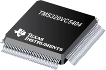
TMS320VC5404 - 数字信号处理器
TMS320VC5404是TI德州仪器公司的一款C5000DSP产品,TMS320VC5404是数字信号处理器,本站介绍了TMS320VC5404的封装应用图解、特点和优点、功能等,并给出了与TMS320VC5404相关的TI元器件型号供参考。
TMS320VC5404 - 数字信号处理器 - C5000DSP - 数字信号处理器 - 德州仪器
This data manual discusses features and specifications of the TMS320VC5407 and TMS320VC5404 (hereafter referred to as the 5407/5404 unless otherwise specified) digital signal processors (DSPs). The 5407 and 5404 are essentially the same device except for differences in their memory maps.
This section lists the pin assignments and describes the function of each pin. This data manual also provides a detailed description section, electrical specifications, parameter measurement information, and mechanical data about the available packaging.
NOTE: This data sheet is designed to be used in conjunction with the TMS320C5000 DSP Family Functional Overview (literature number SPRU307).
The 5407/5404 are based on an advanced modified Harvard architecture that has one program memory bus and three data memory buses. These processors provide an arithmetic logic unit (ALU) with a high degree of parallelism, application-specific hardware logic, on-chip memory, and additional on-chip peripherals. The basis of the operational flexibility and speed of these DSPs is a highly specialized instruction set.
Separate program and data spaces allow simultaneous access to program instructions and data, providing a high degree of parallelism. Two read operations and one write operation can be performed in a single cycle. Instructions with parallel store and application-specific instructions can fully utilize this architecture. In addition, data can be transferred between data and program spaces. Such parallelism supports a powerful set of arithmetic, logic, and bit-manipulation operations that can all be performed in a single machine cycle. These DSPs also include the control mechanisms to manage interrupts, repeated operations, and function calls.
- Advanced Multibus Architecture With Three Separate 16-Bit Data Memory Buses and One Program Memory Bus
- 40-Bit Arithmetic Logic Unit (ALU) Including a 40-Bit Barrel Shifter and Two Independent 40-Bit Accumulators
- 17- × 17-Bit Parallel Multiplier Coupled to a 40-Bit Dedicated Adder for Non-Pipelined Single-Cycle Multiply/Accumulate (MAC) Operation
- Compare, Select, and Store Unit (CSSU) for the Add/Compare Selection of the Viterbi Operator
- Exponent Encoder to Compute an Exponent Value of a 40-Bit Accumulator Value in a Single Cycle
- Two Address Generators With Eight Auxiliary Registers and Two Auxiliary Register Arithmetic Units (ARAUs)
- Data Bus With a Bus Holder Feature
- Extended Addressing Mode for 8M × 16-Bit Maximum Addressable External Program Space
- On-Chip ROM
- 128K × 16-Bit (5407) Configured for Program Memory
- 64K × 16-Bit (5404) Configured for Program Memory
- On-Chip RAM
- 40K × 16-Bit (5407) Composed of Five Blocks of 8K × 16-Bit On-Chip Dual-Access Program/Data RAM
- 16K x 16-Bit (5404) Composed of Two Blocks of 8K × 16-Bit On-Chip Dual-Access Program/Data RAM
- Enhanced External Parallel Interface (XIO2)
- Single-Instruction-Repeat and Block-Repeat Operations for Program Code
- Block-Memory-Move Instructions for Better Program and Data Management
- Instructions With a 32-Bit Long Word Operand
- Instructions With Two- or Three-Operand Reads
- Arithmetic Instructions With Parallel Store and Parallel Load
- Conditional Store Instructions
- Fast Return From Interrupt
- On-Chip Peripherals
- Software-Programmable Wait-State Generator and Programmable Bank-Switching
- On-Chip Programmable Phase-Locked Loop (PLL) Clock Generator With External Clock Source
- Two 16-Bit Timers
- Six-Channel Direct Memory Access (DMA) Controller
- Three Multichannel Buffered Serial Ports (McBSPs)
- 8/16-Bit Enhanced Parallel Host-Port Interface (HPI8/16)
- Universal Asynchronous Receiver/Transmitter (UART) With Integrated Baud Rate Generator
- Power Consumption Control With IDLE1, IDLE2, and IDLE3 Instructions With Power-Down Modes
- CLKOUT Off Control to Disable CLKOUT
- On-Chip Scan-Based Emulation Logic, IEEE Std 1149.1 (JTAG) Boundary Scan Logic
- 144-Pin Ball Grid Array (BGA) (GGU Suffix)
- 144-Pin Low-Profile Quad Flatpack (LQFP) (PGE Suffix)
- 8.33-ns Single-Cycle Fixed-Point Instruction Execution Time (120 MIPS)
- 3.3-V I/O Supply Voltage
- 1.5-V Core Supply Voltage
IEEE Standard 1149.1-1990 Standard-Test-Access Port and Boundary Scan Architecture. All trademarks are the property of their respective owners. TMS320C54x is a trademark of Texas Instruments.
- DS26F32MQML-SP - Quad Differential Line Receivers
- UC2573 - 降压脉宽调制器步降稳压器
- TPS22965-Q1 - 具有控制启动功能的汽车类超低 rON、6A 负载开关
- ADC104S021Q-Q1 - ADC104S021/21Q 4 通道、50 ksps 至 200 ksps、10 位 A/D 转换器
- SN74ALS273 - 具有清零功能的八路 D 类上升沿触发器
- CD74HC190 - 高速 CMOS 逻辑可预置同步 BCD 十进制加/减计数器
- LM2698 - SIMPLE SWITCHER? 1.35A 升压稳压器
- REF2930 - 采用 SOT23-3 封装的 3.0V 100ppm/℃,50uA 系列(带隙)电压基准
- DS42BR400 - 具有发送去加重功能和接收均衡的四路 4.25 Gbps CML 收发器
- TPS76750-Q1 - 汽车类快速瞬态响应 1A 低压降稳压器

