


- SN74LVC00APWG4 - 集成电路(IC) > 逻辑 > 门和反相器
- LM5165QDRCRQ1 - 集成电路(IC) > 电源管理(PMIC) > 稳压器 - DC-DC 开关稳压器
- TPS2034DG4 - 集成电路(IC) > 电源管理(PMIC) > 配电开关,负载驱动器
- F28377DPTPSEP - 集成电路(IC) > 嵌入式 > 微控制器
- LMX2430EVAL/NOPB - 开发板,套件,编程器 > 评估板 > 射频评估和开发套件,板
- SN74HCT04NSR - 集成电路(IC) > 逻辑 > 门和反相器
- MSP430F123IRHBT - 集成电路(IC) > 嵌入式 > 微控制器
- SN74AHCU04PWR - 集成电路(IC) > 逻辑 > 门和反相器
- BQ51013EVM-725 - 开发板,套件,编程器 > 评估板 > 评估和演示板及套件
- SN74AUC1G14YEAR - 逻辑 - 栅极和逆变器
- AM2632CODFHMZCZRQ1 - 集成电路(IC) > 嵌入式 > 微控制器
- SN74ALVC244DWR - 集成电路(IC) > 逻辑 > 缓冲器,驱动器,接收器,收发器
- SN74LS38245DBR - 集成电路(IC) > 逻辑 > 计数器,除法器
- DAC7558IRHBT - 集成电路(IC) > 数据采集 > 数模转换器(DAC)
- CDCFR83DBQRG4 - 集成电路(IC) > 时钟/定时 > 应用特定时钟/定时
- TPS40211EVM-352 - 开发板,套件,编程器 > 评估板 > LED 驱动器评估板
- LP2985A-28DBVRG4 - 集成电路(IC) > 电源管理(PMIC) > 稳压器 - 线性
- SN74LS253DG4 - 逻辑 - 信号开关,多路复用器,解码器
- SN74LV86ATPWRG4Q1 - 集成电路(IC) > 逻辑 > 门和反相器
- BQ294506DRVT - 集成电路(IC) > 电源管理(PMIC) > 电池管理


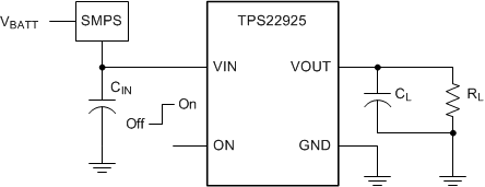
TPS22925 - 3.6V,3A,10mΩ 导通电阻负载开关
TPS22925是TI德州仪器公司的一款配电与蓄电产品,TPS22925是3.6V,3A,10mΩ 导通电阻负载开关,本站介绍了TPS22925的封装应用图解、特点和优点、功能等,并给出了与TPS22925相关的TI元器件型号供参考。
TPS22925 - 3.6V,3A,10mΩ 导通电阻负载开关 - 配电与蓄电 - 集成负载开关 - 德州仪器
- Input Voltage Range: 0.65 V to 3.6 V
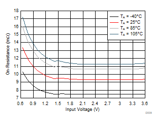
- On-Resistance
- RON = 9.2 mΩ at VIN = 3.6 V
- RON = 9.2 mΩ at VIN = 1.8 V
- RON = 10.2 mΩ at VIN = 1 V
- RON = 13.1 mΩ at VIN = 0.65 V
- 3-A Maximum Continuous Switch Current
- Quiescent Current, IQ,VIN = 29 µA at VIN = 3.6 V
- Low Control Input Threshold Enables 1.5-V, 1.8-V, 2.5-V, or 3.3-V Logic
- Controlled Slew Rate
- tR = 97 µs at VIN = 3.6 V (TPS22925Bx)
- tR = 810 µs at VIN = 3.6 V (TPS22925Cx)
- Reverse Current Blocking (When Disabled)
- Quick Output Discharge (QOD) (TPS22925B and TPS22925C only)
- Wafer Chip Scale Package:
- 0.9 mm x 1.4 mm, 0.5 mm Pitch, 0.4 mm Height
- ESD Performance Tested per JESD 22
- 1 kV HBM and 500 V CDM
- Computing
- SSD
- Tablets
- Wearables
- EPOS
The TPS22925 product family consists of four devices: TPS22925B, TPS22925BN, TPS22925C, and TPS22925CN. Each device is a 9-mΩ, single-channel load switch with a controlled slew rate.
The devices contain an N–channel MOSFET that can operate over an input voltage range of 0.65 V to 3.6V and can support a maximum continuous current of 3 A. This continuous current enables the devices to be used across multiple designs and end equipments. Each of the TPS22925 devices provides reverse current blocking when disabled allowing for power supply protection and power multiplexing capabilities.
The controlled rise time for the device greatly reduces inrush current caused by large bulk load capacitances, thereby reducing or eliminating power supply droop. When operating with an input voltage of 3.6 V, the TPS22925Bx devices feature a 97 μs rise time and the TPS22925Cx devices feature an 810 μs rise time.
The TPS22925 family of devices can help reduce the total solution size by offering an optional integrated, 150-Ω pull–down resistor for quick output discharge (QOD) when the switch is turned off. Each of the TPS22925 devices is available in a 0.9 mm × 1.4 mm, 0.5 mm pitch, 0.4 mm height 6–pin wafer chip scale package (WCSP) allowing for smaller, more integrated designs. The WCSP and 9 mΩ of on-resistance allow use in space constrained, battery powered applications. The device is characterized for operation over the free–air temperature range of –40°C to 105°C.
| PART NUMBER | PACKAGE | BODY SIZE (NOM) |
|---|---|---|
| TPS22925B | DSBGA (6) | 0.90 mm × 1.40 mm |
| TPS22925BN | ||
| TPS22925C | ||
| TPS22925CN |
- DAC811 - 具有并行接口的 12 位数模转换器
- UCD3138A - UCD3138A 用于隔离电源的高度集成数字控制器
- SN54LS684 - 8 位幅度/等值比较器
- LMZ14201EXT - 具有 42V 最大输入电压的 1A SIMPLE SWITCHER 电源模块,用于军事和坚固耐用的应用
- ADS7822-Q1 - 汽车类 12 位 200kSPS 微功耗采样模数转换器
- TL750M05 - 单输出 LDO、750mA、固定电压 (5.0V)、低静态电流、60V 负载突降保护
- LMK04100 - 具有级联 PLL 的精密时钟调节器时钟抖动清洁器
- UCC38C40 - BiCMOS 低功耗电流模式 PWM 控制器
- ADS7953-Q1 - 车用 12 位、1 MSPS、16 通道、单端、微功耗、串行接口、SAR ADC
- SN65LVDS180-Q1 - 汽车类高速差动线路驱动器和接收器

