



- TPS51216RUKR - 集成电路(IC) > 电源管理(PMIC) > 特殊用途稳压器
- LM5155QDSSRQ1 - 集成电路(IC) > 电源管理(PMIC) > DC-DC 开关控制器
- LOG200EVM - 开发板,套件,编程器 > 评估板 > 运算放大器评估板
- SN74HCT240DGSR - 集成电路(IC) > 逻辑 > 缓冲器,驱动器,接收器,收发器
- PTH05050YAZ - 板安装电源 > 直流转换器
- TPS3423GAMDHADRLR - 集成电路(IC) > 电源管理(PMIC) > 监控器
- REF3012AIDBZT - 集成电路(IC) > 电源管理(PMIC) > 电压基准
- UC3842D - 集成电路(IC) > 电源管理(PMIC) > DC-DC 开关控制器
- SN74AHC125QDRQ1 - 集成电路(IC) > 逻辑 > 缓冲器,驱动器,接收器,收发器
- DRV103U/2K5 - 集成电路(IC) > 电源管理(PMIC) > 配电开关,负载驱动器
- SN74HC244NSRG4 - 集成电路(IC) > 逻辑 > 缓冲器,驱动器,接收器,收发器
- AMC0330DQDWVRQ1 - 集成电路(IC) > 线性 > 放大器 > 仪器,运算放大器,缓冲器
- CD4520BPWR - 集成电路(IC) > 逻辑 > 计数器,除法器
- LM337K STEEL/NOPB - 集成电路(IC) > 电源管理(PMIC) > 稳压器 - 线性
- 74ACT11257NSRE4 - 逻辑 - 信号开关,多路复用器,解码器
- TPS51222RTVT - 集成电路(IC) > 电源管理(PMIC) > 稳压器 - 线性 + 开关
- SN6501DBVT - 集成电路(IC) > 电源管理(PMIC) > 电源管理 - 专用
- TPSM84212EVM-888 - 开发板,套件,编程器 > 评估板 > DC/DC 和 AC/DC(离线)SMPS 评估板
- TLV320AIC10CPFB - 集成电路(IC) > 接口 > 编解码器
- UCC2806DWTRG4 - 集成电路(IC) > 电源管理(PMIC) > DC-DC 开关控制器



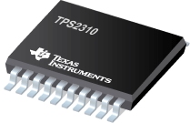
TPS2310 - 具有内部关联的通道电路中断电源状态良好指示报告、工 作态低电平使能输入的 3-13V 双路热交换 IC
TPS2310是TI德州仪器公司的一款热插拔控制器(正48V)产品,TPS2310是具有内部关联的通道电路中断电源状态良好指示报告、工 作态低电平使能输入的 3-13V 双路热交换 IC,本站介绍了TPS2310的封装应用图解、特点和优点、功能等,并给出了与TPS2310相关的TI元器件型号供参考。
TPS2310 - 具有内部关联的通道电路中断电源状态良好指示报告、工 作态低电平使能输入的 3-13V 双路热交换 IC - 热插拔控制器(正48V) - 保护、监控和热插拔 - 德州仪器
The TPS2310 and TPS2311 are dual-channel hot-swap controllers that use external N-channel MOSFETs as high-side switches in power applications. Features of these devices, such as overcurrent protection (OCP), inrush current control, output-power status reporting, and the ability to discriminate between load transients and faults, are critical requirements for hot-swap applications.
The TPS2310/11 devices incorporate undervoltage lockout (UVLO) and power-good (PG) reporting to ensure the device is off at start-up and confirm the status of the output voltage rails during operation. Each internal charge pump, capable of driving multiple MOSFETs, provides enough gate-drive voltage to fully enhance the N-channel MOSFETs. The charge pumps control both the rise times and fall times (dv/dt) of the MOSFETs, reducing power transients during power up/down. The circuit-breaker functionality combines the ability to sense overcurrent conditions with a timer function; this allows designs such as DSPs, that may have high peak currents during power-state transitions, to disregard transients for a programmable period.
DISCH1, DISCH2–DISCH1 and DISCH2 should be connected to the sources of the external N-channel MOSFET transistors connected to GATE1 and GATE2, respectively. These pins discharge the loads when the MOSFET transistors are disabled. They also serve as reference-voltage connections for internal gate voltage-clamp circuitry.
ENABLE or ENABLE–ENABLE for TPS2310 is active-low. ENABLE for TPS2311 is active-high. When the controller is enabled, both GATE1 and GATE2 voltages will power up to turn on the external MOSFETs. When the ENABLE pin is pulled high for TPS2310 or the ENABLE pin is pulled low for TPS2311 for more than 50 µs, the gate of the MOSFET is discharged at a controlled rate by a current source, and a transistor is enabled to discharge the output bulk capacitance. In addition, the device turns on the internal regulator PREREG (see VREG) when enabled and shuts down PREREG when disabled so that total supply current is less than 5 µA.
FAULT –FAULT is an open-drain overcurrent flag output. When an overcurrent condition in either channel is sustained long enough to charge TIMER to 0.5 V, both channels latch off and pull this pin low. In order to turn the device back on, either the enable pin has to be toggled or the input power has to be cycled.
GATE1, GATE2– GATE1 and GATE2 connect to the gates of external N-channel MOSFET transistors. When the device is enabled, internal charge-pump circuitry pulls these pins up by sourcing approximately 15 µA to each. The turnon slew rates depend upon the capacitance present at the GATE1 and GATE2 terminals. If desired, the turnon slew rates can be further reduced by connecting capacitors between these pins and ground. These capacitors also reduce inrush current and protect the device from false overcurrent triggering during powerup. The charge-pump circuitry generates gate-to-source voltages of 9 V–12 V across the external MOSFET transistors.
IN1, IN2– IN1 and IN2 should be connected to the power sources driving the external N-channel MOSFET transistors connected to GATE1 and GATE2, respectively. The TPS2310/TPS2311 draws its operating current from IN1, and both channels remains disabled until the IN1 power supply has been established. The IN1 channel has been constructed to support 3-V, 5-V, or 12-V operation, while the IN2 channel has been constructed to support 3-V or 5-V operation
ISENSE1, ISENSE2, ISET1, ISET2–ISENSE1 and ISENSE2, in combination with ISET1 and ISET2, implement overcurrent sensing for GATE1 and GATE2. ISET1 and ISET2 set the magnitude of the current that generates an overcurrent fault, through external resistors connected to ISET1 and ISET2. An internal current source draws 50 µA from ISET1 and ISET2. With a sense resistor from IN1 to ISENSE1 or from IN2 to ISENSE2, which is also connected to the drains of external MOSFETs, the voltage on the sense resistor reflects the load current. An overcurrent condition is assumed to exist if ISENSE1 is pulled below ISET1 or if ISENSE2 is pulled below ISET2. To ensure proper circuit breaker operation, VI(ISENSE1) and VI(ISET1) should never exceed VI(IN1). Similarly, VI(ISENSE2) and VI(ISET2) should never exceed VI(IN2).
PWRGD1, PWRGD2–PWRGD1 and PWRGD2 signal the presence of undervoltage conditions on VSENSE1 and VSENSE2, respectively. These pins are open-drain outputs and are pulled low during an undervoltage condition. To minimize erroneous PWRGDx responses from transients on the voltage rail, the voltage sense circuit incorporates a 20-µs deglitch filter. When VSENSEx is lower than the reference voltage (about 1.23 V), PWRGDx is active low to indicate an undervoltage condition on the power-rail voltage. PWRGDx may not correctly report power conditions when the device is disabled, because there is no gate drive power for the PWRGD output transistor in the disable mode, or, in other words, PWRGD is floating. Therefore, PWRGD is pulled up to its pullup power supply rail in disable mode.
TIMER–A capacitor on TIMER sets the time during which the power switch can be in overcurrent before turning off. When the overcurrent protection circuits sense an excessive current, a current source is enabled which charges the capacitor on TIMER. Once the voltage on TIMER reaches approximately 0.5 V, the circuit-breaker latch is set and the power switch is latched off. Power must be recycled or the ENABLE pin must be toggled to restart the controller. In high-power or high-temperature applications, a minimum 50-pF capacitor is strongly recommended from TIMER to ground, to prevent any false triggering.
VREG–VREG is the output of an internal low-dropout voltage regulator, where IN1 is the input. The regulator is used to generate a regulated voltage source, less than 5.5 V, for the device. A 0.1-µF ceramic capacitor should be connected between VREG and ground to aid in noise rejection. In this configuration, upon disabling the device, the internal low-dropout regulator will also be disabled, which removes power from the internal circuitry and allows the device to be placed in low-quiescent-current mode. In applications where IN1 is less than 5.5 V, VREG and IN1 may be connected together. However, under these conditions, disabling the device does not place the device in low-quiescent-current mode, because the internal low-dropout voltage regulator is being bypassed, thereby keeping internal circuitry operational. If VREG and IN1 are connected together, a 0.1-µF ceramic capacitor between VREG and ground is not needed if IN1 already has a bypass capacitor of 1 µF to 10µF.
VSENSE1, VSENSE2–VSENSE1 and VSENSE2 can be used to detect undervoltage conditions on external circuitry. If VSENSE1 senses a voltage below approximately 1.23 V, PWRGD1 is pulled low. Similarly, a voltage less than 1.23 V on VSENSE2 causes PWRGD2 to be pulled low.
- Dual-Channel High-Side MOSFET Drivers
- IN1: 3 V to 13 V; IN2: 3 V to 5.5 V
- Output dV/dt Control Limits Inrush Current
- Circuit-Breaker With Programmable Overcurrent Threshold and Transient Timer
- Power-Good Reporting With Transient Filter
- CMOS- and TTL-Compatible Enable Input
- Low, 5-µA Standby Supply Current .(Max)
- Available in 20-Pin TSSOP Package
- –40°C to 85°C Ambient Temperature Range
- Electrostatic Discharge Protection
- UC1856 - 改进的电流模式 PWM 控制器
- BQ771800 - 用于 2 至 5 节锂离子电池(具有内部延迟定时器)的过压保护
- TL4051B12 - 精密微功耗并联电压基准
- DLPC3438 - 低功耗 DLP 显示控制器
- ISO7631FC - 4kVpk 低功耗三通道、25Mbps 数字隔离器
- TPIC1021A-Q1 - 汽车类 LIN 物理接口
- TSC2008-Q1 - 具有 SPI 的汽车类毫微功率触摸屏控制器
- ADS7841-Q1 - 汽车类 12 位、4 通道串行输出采样模数转换器
- LM27966 - 具有 I2C 兼容接口的白光 LED 驱动器
- TMP124 - 具有 SPI 接口的 ±1°C 温度传感器,支持报警功能,采用 SOIC 封装

