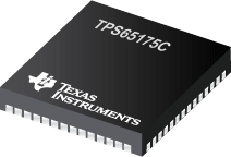

TPS65175C是TI公司的一款电流感应放大器、I2C/PMBus监控器产品,TPS65175C是完全可编程 LCD 偏置 IC,用于具有 12 通道电平转换器和伽马缓冲器的 GIP TV,本页介绍了TPS65175C的产品说明、应用、特性等,并给出了与TPS65175C相关的TI元器件型号供参考。
TPS65175C - 完全可编程 LCD 偏置 IC,用于具有 12 通道电平转换器和伽马缓冲器的 GIP TV - 电流感应放大器、I2C/PMBus监控器 - 保护、监控和热插拔 - TI公司(Texas Instruments,德州仪器)
The TPS65175B/C provides a simple and economic power supply solution for a wide variety of LCD bias applications. The device provides all supply rails needed by a TFT-LCD panel but also 6 gamma references, a supply rail for LVDS support, as well as a Vcom reference. The device also integrates a VCOM_DAC rail providing the reference for an external non-inverting operational amplifier input. A 12-Channel Level Shifter is also integrated. The solution is delivered in a small 7×7 mm QFN package.
The TPS65175B/C provides a simple and economic power supply solution for a wide variety of LCD bias applications. The device provides all supply rails needed by a TFT-LCD panel. VCC and RST for the T-Con. VDD and HVDD for the Source Driver. VGH and VGL for the Gate Driver or the Level Shifters. A VCOM operational amplifier is also integrated to provide a common plane reference. The VGH and VCOM / VCOM_DAC voltages can be compensated for low and high temperatures. The transition from one programmed value to another is made using an external thermistor connected to the IC. In addition, a 6-channel Gamma Buffer as well as a 12-Channel Level Shifter are integrated. All output rails and delay times are programmable by a two-wire interface: a single BOM (Bill of Material) can cover several panel types and sizes whose desired output levels can be programmed in production and stored in a non-volatile memory embedded into the TPS65175B/C. The solution is delivered in a small 7 mm × 7 mm QFN-56 package.
- 8.6V to 14.7V Input Voltage Range
- Boost Converter VDD: 12.7V…19V (6-Bit)
- Integrated Input-to-Output Isolation Switch
- Buck Converter HVDD: VDD Tracking
- Buck Converter VCC: 1.6V...2.0V & 3.0V…3.6V (4-Bit)
- Positive Charge Pump VGH:
- 19V…34V for Low Temperature (4-Bit)
- 17V…32V for High Temperature (4-Bit)
- Negative Charge Pump VGL: –1.8V…–8.1V (6-Bit)
- 6-Ch Gamma Buffer:
- 3-Ch: VDD…HVDD (9-Bit)
- 3-Ch: HVDD...GND (9-Bit)
- 9-Bit VCOM Reference
- 3-Bit VCOM Gain
- VCOM_DAC Output for External Operational Amplifier Reference
- Temperature Compensation for VGH and VCOM
- Reset Signal with Programmable Delay Time
- Programmable Sequencing Delays (4 × 3-Bit)
- Thermal Shutdown
- 12-Channel Level Shifters:
- Supports Forward and Reverse Operation
- Abnormal Operation Detection
- 56-Pin 7-mm × 7-mm QFN Package


