


- DAC8234SPFB - 集成电路(IC) > 数据采集 > 数模转换器(DAC)
- SNJ54BCT373J - 集成电路(IC) > 逻辑 > 锁存器
- TS3L110PWRG4 - 集成电路(IC) > 接口 > 模拟开关 - 特殊用途
- SN74LV04ADRG4 - 集成电路(IC) > 逻辑 > 门和反相器
- TL082ACPS - 集成电路(IC) > 线性 > 放大器 > 仪器,运算放大器,缓冲器
- BQ4845S-A4NTR - 集成电路(IC) > 时钟/定时 > 实时时钟
- DAC5686EVM - 开发板,套件,编程器 > 评估板 > 数模转换器(DAC)评估板
- PT4413A - 板安装电源 > 直流转换器
- TPS650245RHBT - 集成电路(IC) > 电源管理(PMIC) > 电池管理
- AFE2256TDT - 集成电路(IC) > 数据采集 > 模拟前端(AFE)
- OPA360AIDCKTG4 - 集成电路(IC) > 线性 > 放大器 > 视频放大器和模块
- SN75183DE4 - 集成电路(IC) > 接口 > 驱动器,接收器,收发器
- UCC28600EVM - 开发板,套件,编程器 > 评估板 > DC/DC 和 AC/DC(离线)SMPS 评估板
- LM2574M-ADJ - 集成电路(IC) > 电源管理(PMIC) > 稳压器 - DC-DC 开关稳压器
- DAC7554IDGS - 集成电路(IC) > 数据采集 > 数模转换器(DAC)
- LMK05318EVM - 开发板,套件,编程器 > 评估板 > 评估和演示板及套件
- TAS5508APAGR - 集成电路(IC) > 音频专用
- ADC102S051CIMMX - 数据采集 - 模数转换器(ADC)
- LM317S/NOPB - 集成电路(IC) > 电源管理(PMIC) > 稳压器 - 线性
- LM2671LD-3.3/NOPB - 电源管理IC - 稳压器 - DC DC 开关稳压器


UCC27531-Q1 - UCC27531-Q1 2.5A、5A、35VMAX VDD FET 和 IGBT 单门驱动器
UCC27531-Q1是TI德州仪器公司的一款低侧驱动器产品,UCC27531-Q1是UCC27531-Q1 2.5A、5A、35VMAX VDD FET 和 IGBT 单门驱动器,本站介绍了UCC27531-Q1的封装应用图解、特点和优点、功能等,并给出了与UCC27531-Q1相关的TI元器件型号供参考。
UCC27531-Q1 - UCC27531-Q1 2.5A、5A、35VMAX VDD FET 和 IGBT 单门驱动器 - 低侧驱动器 - MOSFET和IGBT栅极驱动器 - 德州仪器
- Qualified for Automotive Applications
- AEC-Q100 Qualified with the Following Results:
- Device Temperature Grade 1
- Device HBM ESD Classification Level H2
- Device CDM ESD Classification Level C4B
- Low Cost Gate Driver (Offering Optimal Solution for Driving Fet And Igbts)
- Superior Replacement to Discrete Transistor Pair Drive (Providing Easy Interface With Controller)
- TTL and CMOS Compatible Input Logic Threshold, (Independent of Supply Voltage)
- Split Output Options Allow for Tuning of Turn-On and Turn-Off Currents
- Enable with Fixed TTL Compatible Threshold
- High 2.5-A Source and 5-A Sink Peak Drive Currents at 18-V VDD
- Wide VDD Range From 10 V up to 35 V
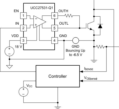
- Input and Enable Pins Capable of Withstanding up to –5-V DC Below Ground
- Output Held Low When Inputs are Floating or During VDD UVLO
- Fast Propagation Delays (17-ns Typical)
- Fast Rise and Fall Times (15-ns and 7-ns Typical With 1800-pF Load)
- Undervoltage Lockout (UVLO)
- Used as a High-Side or Low-Side Driver (if Designed With Proper Bias and Signal Isolation)
- Low-Cost, Space-Saving 6-Pin DBV (SOT-23) Package Options
- Operating Temperature Range of –40°C to 140°C
- Automotive
- Switch-Mode Power Supplies
- DC-to-DC Converters
- Solar Inverters, Motor Control, UPS
- HEV and EV Chargers
- Home Appliances
- Renewable Energy Power Conversion
- SiC FET Converters
The UCC27531-Q1 is a single-channel, high-speed, gate driver capable of effectively driving MOSFET and IGBT power switches by using up to 2.5-A source and 5-A sink (asymmetrical drive) peak current. Strong sink capability in asymmetrical drive boosts immunity against parasitic Miller turn-on effect. The UCC27531-Q1 device can also feature a split-output configuration where the gate-drive current is sourced through the OUTH pin and sunk through the OUTL pin. This pin arrangement allows the user to apply independent turn-on and turn-off resistors to the OUTH and OUTL pins respectively and easily control the switching slew rates.
The driver has rail-to-rail drive capability and an extremely small propagation delay of typically 17 ns.
The input threshold of UCC27531-Q1 is based on TTL and CMOS compatible low-voltage logic, which is fixed and independent of VDD supply voltage. The 1-V typical hysteresis offers excellent noise immunity.
| PART NUMBER | PACKAGE | BODY SIZE (NOM) |
|---|---|---|
| UCC27531-Q1 | SOT-23 (6) | 1.6 mm × 2.9 mm |
- TPS76827-Q1 - 汽车类单输出 LDO、1.0A、固定电压 (2.7V)、低静态电流
- BQ771807 - 具有内部延迟定时器的 2-5S 过压保护器
- TPS22901 - 3.6V,0.5A,78mΩ 负载开关
- TPS51117 - 针对轻载效率优化的具有 DCAP? 模式的 1.8V 至 28V 输入同步 降压控制器
- TL971 - TL971, TL972, TL974
- SN65LBC176 - 差动总线收发器
- TPS62093 - 具有 DCS 控制系统的 3A、2.5V 至 6V 输入同步降压转换器,效率高达 97%
- TPS2159 - 用于 USB 集线器的 3.3V LDO + 双路开关,工作态高电平启用
- LM317L - 3/8 引脚 100mA 可调节正电压稳压器
- TMS320F2801 - 具有闪存的 32 位数字信号控制器

