


- LM5025CMTC/NOPB - 集成电路(IC) > 电源管理(PMIC) > DC-DC 开关控制器
- TPS2010APWPG4 - 电源管理IC - 配电开关,负载驱动器
- MSP430F2121TDWR - 集成电路(IC) > 嵌入式 > 微控制器
- DS90CR285MTDX/NOPB - 集成电路(IC) > 接口 > 专用
- TLV2453AIDR - 集成电路(IC) > 线性 > 放大器 > 仪器,运算放大器,缓冲器
- SN74ABT861NT - 集成电路(IC) > 逻辑 > 缓冲器,驱动器,接收器,收发器
- LP2980IBPX-5.0 - 集成电路(IC) > 电源管理(PMIC) > 稳压器 - 线性
- AM2632COKFHAZCZR - 集成电路(IC) > 嵌入式 > 微控制器
- TPS7A8001DRBT - 集成电路(IC) > 电源管理(PMIC) > 稳压器 - 线性
- TDA4VPE6T5AANDRQ1 - 集成电路(IC) > 嵌入式 > 微处理器
- TLV3501AIDBVRG4 - 集成电路(IC) > 线性 > 比较器
- TLC27L4BCNS - 集成电路(IC) > 线性 > 放大器 > 仪器,运算放大器,缓冲器
- LM3S3N26-IQR50-C3 - 集成电路(IC) > 嵌入式 > 微控制器
- LP2951ACMMX/NOPB - 集成电路(IC) > 电源管理(PMIC) > 稳压器 - 线性
- ADS8328IRSAT - 集成电路(IC) > 数据采集 > 模数转换器(ADC)
- TPS7A8401ARGRR - 集成电路(IC) > 电源管理(PMIC) > 稳压器 - 线性
- TLV70236QDSERQ1 - 集成电路(IC) > 电源管理(PMIC) > 稳压器 - 线性
- CD4009UBNSRE4 - 逻辑 - 栅极和逆变器
- LP5912Q1.1DRVTQ1 - 集成电路(IC) > 电源管理(PMIC) > 稳压器 - 线性
- MSP430F2274TDAR - 集成电路(IC) > 嵌入式 > 微控制器


CDC3RL02 - 双通道方波/正弦-方波时钟缓冲器
CDC3RL02是TI德州仪器公司的一款单端产品,CDC3RL02是双通道方波/正弦-方波时钟缓冲器,本站介绍了CDC3RL02的封装应用图解、特点和优点、功能等,并给出了与CDC3RL02相关的TI元器件型号供参考。
CDC3RL02 - 双通道方波/正弦-方波时钟缓冲器 - 单端 - 时钟缓冲器 - 德州仪器
- Low Additive Noise:
- –149 dBc/Hz at 10-kHz Offset Phase Noise
- 0.37 ps (RMS) Output Jitter
- Limited Output Slew Rate for EMI Reduction (1- to 5-ns/Rise/Fall Time for 10-pF to 50-pF Loads)
- Adaptive Output Stage Controls Reflection
- Regulated 1.8-V Externally Available I/O Supply
- Ultra-Small 8-bump YFP 0.4-mm Pitch WCSP (0.8 mm × 1.6 mm)
- ESD Performance Exceeds JESD 22
- 2000-V Human-Body Model (A114-A)
- 1000-V Charged-Device Model (JESD22-C101-A Level III)
- Cellular Phones
- Global Positioning Systems (GPS)
- Wireless LAN
- FM Radio
- WiMAX
- W-BT
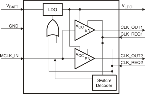
The CDC3RL02 is a two-channel clock fan-out buffer. It buffers a single master clock, such as a temperature compensated crystal oscillator (TCXO) to multiple peripherals. The device has two clock request inputs (CLK_REQ1 and CLK_REQ2), each of which enable a single clock output.
The CDC3RL02 accepts square or sine waves at the master clock input (MCLK_IN), eliminating the need for an AC coupling capacitor. The smallest acceptable sine wave is a 0.3-V signal (peak-to-peak). CDC3RL02 has been designed to offer minimal channel-to-channel skew, additive output jitter, and additive phase noise. The adaptive clock output buffers offer controlled slew-rate over a wide capacitive loading range which minimizes EMI emissions, maintains signal integrity, and minimizes ringing caused by signal reflections on the clock distribution lines.
The CDC3RL02 has an integrated Low-Drop-Out (LDO) voltage regulator which accepts input voltages from 2.3 V to 5.5 V and outputs 1.8 V, 50 mA. This 1.8V supply is externally available to provide regulated power to peripheral devices such as a TCXO.
The CDC3RL02 is ideal for use in portable end-equipment, such as mobile phones, that require clock buffering with minimal additive phase noise and fan-out capabilities. It is offered in a 0.4-mm pitch wafer-level chip-scale (WCSP) package (0.8 mm × 1.6 mm) and is optimized for very low standby current consumption.
| PART NUMBER | PACKAGE | BODY SIZE (NOM) |
|---|---|---|
| CDC3RL02 | DSBGA (8) | 0.80 mm × 1.60 mm |
- TPS62650 - 采用芯片级封装的 800mA、6MHz 同步降压转换器
- SN54ALS138A - 3 线路至 8 线路解码器/多路解复用器
- LM27313-Q1 - 具有 30V 内部 FET 开关(采用 SOT-23 封装)的 1.6 MHz 升压转换器
- TL16C554A - 具有 16 字节 FIFO 的四路 UART
- MSP430F6736A - MSP430F673xA 和MSP430F672xA 混合信号微控制器
- TPS62262 - 采用 2x2mm SON/TSOT23 封装的 2.25MHz 600mA 降压转换器
- LM4930 - 具有立体声耳机和单声道扬声器放大器的音频子系统
- BQ2057C - 锂离子低压降线性 (4.2V) 充电管理 IC,用于具有 AutoCompTM 的 1 节应用领域
- LMK61A2-312M - 超低抖动固定频率差分振荡器 - 312M50
- CD54HCT166 - 高速 CMOS 逻辑 8 位并行输入/串行输出移位寄存器

