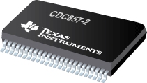

CDC857-2是TI公司的一款DDRPLL产品,CDC857-2是锁相环时钟驱动器,本页介绍了CDC857-2的产品说明、应用、特性等,并给出了与CDC857-2相关的TI元器件型号供参考。
CDC857-2 - 锁相环时钟驱动器 - DDRPLL - 存储器接口时钟和寄存器 - TI公司(Texas Instruments,德州仪器)
The CDC857-2 and CDC857-3 are high-performance, low-skew, low-jitter, phase-lock loop (PLL) clock driver. They use a PLL to precisely align, in both frequency and phase, the feedback (FBOUT) output to the clock (CLK) input signal. The CDC857-3 operates at 3.3 V (PLL) and 2.5 V (output buffer). The CDC857-2 operates at 2.5 V (PLL and output buffer).
One bank of ten inverting and noninverting outputs provide ten low-skew, low-jitter copies of CLK. Output signal duty cycles are adjusted to 50%, independent of the duty cycle at CLK.
All outputs can be enabled or disabled via a single output enable input. When the G input is high, the outputs switch in phase and frequency with CLK; when the G input is low, the outputs are disabled to high impedance state (3-state).
Unlike many products containing PLLs, the CDC857 does not require external RC networks. The loop filter for the PLL is included on-chip, minimizing component count, board space, and cost.
Because it is based on PLL circuity, the CDC857 requires a stabilization time to achieve phase lock of the feedback signal to the reference signal. This stabilization time is required following power up and application of a fixed-frequency, fixed-phase signal at CLK, as well as following any changes to the PLL reference or feedback signals. The PLL can be bypassed for test purposes by strapping AVCC to ground. If AVCC is at GND and VCC = ON, 2 falling edges on G cause the PLL to run with FBOUT being enabled and all other outputs being disabled, after AVCC ramps up to its specified VCC value, with G being kept low. The CDC857 is characterized for operation from 0°C to 85°C.
- Phase-Lock Loop Clock Distribution for Double Data Rate Synchronous DRAM Applications
- Distributes One Differential Clock Input to Ten Differential Outputs
- External Feedback Pins (FBIN, FBIN\) Are Used to Synchronize the Outputs to the Clock Input
- Operates at VCC = 2.5 V and AVCC = 3.3 V
- Packaged in Plastic 48-Pin (DGG) Thin Shrink Small-Outline Package (TSSOP)
- Spread Spectrum Clocking Tracking Capability to Reduce EMI


