



- TRS3243EIPWR - 集成电路(IC) > 接口 > 驱动器,接收器,收发器
- LMZ10503TZ-ADJ/NOPB - 板安装电源 > 直流转换器
- LMV934MA - 集成电路(IC) > 线性 > 放大器 > 仪器,运算放大器,缓冲器
- SN74HCS165QBQBRQ1 - 集成电路(IC) > 逻辑 > 移位寄存器
- PT79SR105T - 板安装电源 > 直流转换器
- SN74HC27DR - 集成电路(IC) > 逻辑 > 门和反相器
- 5962-8681301RA - 集成电路(IC) > 逻辑 > 缓冲器,驱动器,接收器,收发器
- JM4013BBDA - 集成电路(IC) > 逻辑 > 触发器
- SN752232DL - 接口 - 驱动器,接收器,收发器
- OPA859QDSGRQ1 - 集成电路(IC) > 线性 > 放大器 > 仪器,运算放大器,缓冲器
- LMG3411R070RWHT - 集成电路(IC) > 电源管理(PMIC) > 配电开关,负载驱动器
- MC34063ADRJRG4 - 集成电路(IC) > 电源管理(PMIC) > 稳压器 - DC-DC 开关稳压器
- SN74LVC8T245PWRE4 - 集成电路(IC) > 逻辑 > 缓冲器,驱动器,接收器,收发器
- TPS61060DRBRG4 - 集成电路(IC) > 电源管理(PMIC) > LED 驱动器
- SN74AUC1G08YZPR - 集成电路(IC) > 逻辑 > 门和反相器
- SNJ5403W - 集成电路(IC) > 逻辑 > 门和反相器
- OPA2677T/2K5 - 集成电路(IC) > 线性 > 放大器 > 仪器,运算放大器,缓冲器
- TPS40210DGQ - 集成电路(IC) > 电源管理(PMIC) > DC-DC 开关控制器
- SN74LVC10ANS - 集成电路(IC) > 逻辑 > 门和反相器
- DRV5032FBDBZR - 传感器,变送器 > 磁性传感器 > 开关(固态)



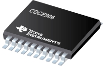
CDCE906 - 可编程 3-PLL 时钟合成器/乘法器/除法器
CDCE906是TI德州仪器公司的一款扩频时钟产品,CDCE906是可编程 3-PLL 时钟合成器/乘法器/除法器,本站介绍了CDCE906的封装应用图解、特点和优点、功能等,并给出了与CDCE906相关的TI元器件型号供参考。
CDCE906 - 可编程 3-PLL 时钟合成器/乘法器/除法器 - 扩频时钟 - 时钟发生器 - 德州仪器
The CDCE906 is one of the smallest and powerful PLL synthesizer / multiplier / divider available today. Despite its small physical outlines, the CDCE906 is flexible. It has the capability to produce an almost independent output frequency from a given input frequency.
The input frequency can be derived from a LVCMOS, differential input clock, or a single crystal. The appropriate input waveform can be selected via the SMBus data interface controller.
To achieve an independent output frequency the reference divider M and the feedback divider N for each PLL can be set to values from 1 up to 511 for the M-Divider and from 1 up to 4095 for the N-Divider. The PLL-VCO (voltage controlled oscillator) frequency than is routed to the free programmable output switching matrix to any of the six outputs. The switching matrix includes an additional 7-bit post-divider (1-to-127) and an inverting logic for each output.
The deep M/N divider ratio allows the generation of zero ppm clocks from any reference input frequency (e.g., a 27 MHz).
The CDCE906 includes three PLLs of those one supports SSC (spread-spectrum clocking). PLL1, PLL2, and PLL3 are designed for frequencies up to 167 MHz and optimized for zero-ppm applications with wide divider factors.
PLL2 also supports center-spread and down-spread spectrum clocking (SSC). This is a common technique to reduce electro-magnetic interference. Also, the slew-rate controllable (SRC) output edges minimize EMI noise.
Based on the PLL frequency and the divider settings, the internal loop filter components will be automatically adjusted to achieve high stability and optimized jitter transfer characteristic of the PLL.
The device supports non-volatile EEPROM programming for easy-customized application. It is preprogrammed with a factory default configuration (see Figure 13) and can be reprogrammed to a different application configuration before it goes onto the PCB or reprogrammed by in-system programming. A different device setting is programmed via the serial SMBus interface.
Two free programmable inputs, S0 and S1, can be used to control for each application the most demanding logic control settings (outputs disable to low, outputs 3-state, power down, PLL bypass, etc).
The CDCE906 has three power supply pins, VCC, VCCOUT1 and VCCOUT2. VCC is the power supply for the device. It operates from a single 3.3-V supply voltage. VCCOUT1 and VCCOUT2 are the power supply pins for the outputs. VCCOUT1 supplies the outputs Y0 and Y1 and VCCOUT2 supplies the outputs Y2, Y3, Y4, and Y5. Both outputs supplies can be 2.3 V to 3.6 V. At output voltages lower than 3.3 V, the output drive current is limited.
The CDCE906 is characterized for operation from 0°C to 70°C.
- High Performance 3:6 PLL based Clock Synthesizer / Multiplier / Divider
- User Programmable PLL Frequencies
- EEPROM Programming Without the Need to Apply High Programming Voltage
- Easy In-Circuit Programming via SMBus Data Interface
- Wide PLL Divider Ratio Allows 0-ppm Output Clock Error
- Generates Precise Video (27 MHz or 54 MHz) and Audio System Clocks from Multiple Sampling Frequencies (fS = 16, 22.05, 24, 32, 44.1, 48, 96 kHz)
- Clock Inputs Accept a Crystal or a Single-Ended LVCMOS or a Differential Input Signal
- Accepts Crystal Frequencies from 8 MHz up to 54 MHz
- Accepts LVCMOS or Differential Input Frequencies up to 167 MHz
- Two Programmable Control Inputs [S0/S1, A0/A1] for User Defined Control Signals
- Six LVCMOS Outputs with Output Frequencies up to 167 MHz
- LVCMOS Outputs can be Programmed for Complementary Signals
- Free Selectable Output Frequency via Programmable Output Switching Matrix [6x6] Including 7-Bit Post-Divider for Each Output
- PLL Loop Filter Components Integrated
- Low Period Jitter (Typ 60 ps)
- Features Spread Spectrum Clocking (SSC) for Lowering System EMI
- Programmable Center Spread SSC Modulation (±0.1%, ±0.25%, and ±0.4%) with a Mean Phase Equal to the Phase of the Non-Modulated Frequency
- Programmable Down Spread SSC Modulation (1%, 1.5%, 2%, and 3%)
- Programmable Output Slew-Rate Control (SRC) for Lowering System EMI
- 3.3-V Device Power Supply
- Commercial Temperature Range 0°C to 70°C
- Development and Programming Kit for Easy PLL Design and Programming (TI Pro-Clock™)
- Packaged in 20-Pin TSSOP
Pro-Clock is a trademark of Texas Instruments.
- TFP401A-Q1 - TI PanelBus ? 数字接收器...
- LP3990-Q1 - 用于数字应用的 150mA 线性电压稳压器
- EMB1428Q - EMB1428Q 开关矩阵栅极驱动器
- DCH010512D - 微型 2W 隔离式未稳压 DC/DC 转换器
- UCD9081 - 电源序列发生器和监控器
- OPA2604 - 双路 FET 输入、低失真运算放大器
- LP3913 - 面向基于闪存的便携式媒体播放器的电源管理 IC (PMIC)
- SN74AUP1G58 - 低功耗可配置多功能门
- LM20343 - 具有可调频率的 4.5-36V、3A 电流模式同步降压稳压器
- CD4011UB - CMOS 四路 2 输入与非门

