


- TPS2350EVM - 开发板,套件,编程器 > 评估板 > 评估和演示板及套件
- LMK3H0102T17RGTRQ1 - 集成电路(IC) > 时钟/定时 > 时钟发生器,PLL,频率合成器
- LMS202EIMX/NOPB - 集成电路(IC) > 接口 > 驱动器,接收器,收发器
- SN74ALVC125NSR - 集成电路(IC) > 逻辑 > 缓冲器,驱动器,接收器,收发器
- TLC1549IP - 集成电路(IC) > 数据采集 > 模数转换器(ADC)
- TSC2100EVM - 开发板,套件,编程器 > 评估板 > 评估和演示板及套件
- LDC0851HDSGR - 传感器,变送器 > 接近传感器
- MSP430F47196IPZR - 集成电路(IC) > 嵌入式 > 微控制器
- UCC21520EVM-286 - 开发板,套件,编程器 > 评估板 > 评估和演示板及套件
- SN74AHC244QPWRG4Q1 - 集成电路(IC) > 逻辑 > 缓冲器,驱动器,接收器,收发器
- PT4224A - 板安装电源 > 直流转换器
- LP2987IMX-3.0/NOPB - 集成电路(IC) > 电源管理(PMIC) > 稳压器 - 线性
- LMZ10500SILT - 板安装电源 > 直流转换器
- TL751M12CKTGR - 集成电路(IC) > 电源管理(PMIC) > 稳压器 - 线性
- LM236DE4-2-5 - 集成电路(IC) > 电源管理(PMIC) > 电压基准
- SN74CB3Q16811DGVR - 集成电路(IC) > 逻辑 > 信号开关,多路复用器,解码器
- LM64460BPPQRYFRQ1 - 集成电路(IC) > 电源管理(PMIC) > 稳压器 - DC-DC 开关稳压器
- THS4531AIDGK - 集成电路(IC) > 线性 > 放大器 > 仪器,运算放大器,缓冲器
- LMH6553MRX/NOPB - 集成电路(IC) > 线性 > 放大器 > 仪器,运算放大器,缓冲器
- TS3DV621RUAR - 集成电路(IC) > 线性 > 视频处理


CDCM7005 - 高性能、低相位噪声、低偏移的时钟同步器(使参考时钟与 VCXO 同步)
CDCM7005是TI德州仪器公司的一款单回路PLL产品,CDCM7005是高性能、低相位噪声、低偏移的时钟同步器(使参考时钟与 VCXO 同步),本站介绍了CDCM7005的封装应用图解、特点和优点、功能等,并给出了与CDCM7005相关的TI元器件型号供参考。
CDCM7005 - 高性能、低相位噪声、低偏移的时钟同步器(使参考时钟与 VCXO 同步) - 单回路PLL - 时钟抖动消除器 - 德州仪器
- High Performance LVPECL and LVCMOS PLL Clock Synchronizer
- Two Reference Clock Inputs (Primary and Secondary Clock) for Redundancy Support With Manual or Automatic Selection
- Accepts LVCMOS Input Frequencies up to 200 MHz
- VCXO_IN Clock is Synchronized to One of the Two Reference Clocks
- VCXO_IN Frequencies Up to 2.2 GHz (LVPECL)
- Outputs Can Be a Combination of LVPECL and LVCMOS (Up to Five Differential LVPECL Outputs or up to 10 LVCMOS Outputs)
- Output Frequency is Selectable by ×1, /2, /3, /4, /6, /8, /16 on Each Output Individually
- Efficient Jitter Cleaning From Low PLL Loop Bandwidth
- Low Phase Noise PLL Core
- Programmable Phase Offset (PRI_REF and SEC_REF to Outputs)
- Wide Charge Pump Current Range From 200 μA to 3 mA
- Dedicated Charge Pump Supply (VCC_CP) for Wide Tuning Voltage Range VCOs
- Presets Charge Pump to VCC_CP/2 for Fast Center-Frequency Setting of VC(X)O
- Analog and Digital PLL Lock Indication
- Provides VBB Bias Voltage Output for Single-Ended Input Signals (VCXO_IN)
- Frequency Hold-Over Mode Improves Fail-Safe Operation
- Power-up Control Forces LVPECL Outputs to 3-State at VCC < 1.5 V
- SPI Controllable Device Setting
- 3.3-V Power Supply
- Packaged in 64-Pin BGA (0.8 mm Pitch – ZVA) or 48-Pin QFN (RGZ)
- Industrial Temperature Range –40°C to 85°C
- Wireless Infrastructure
- SONET
- Data Communication
- Test Equipment
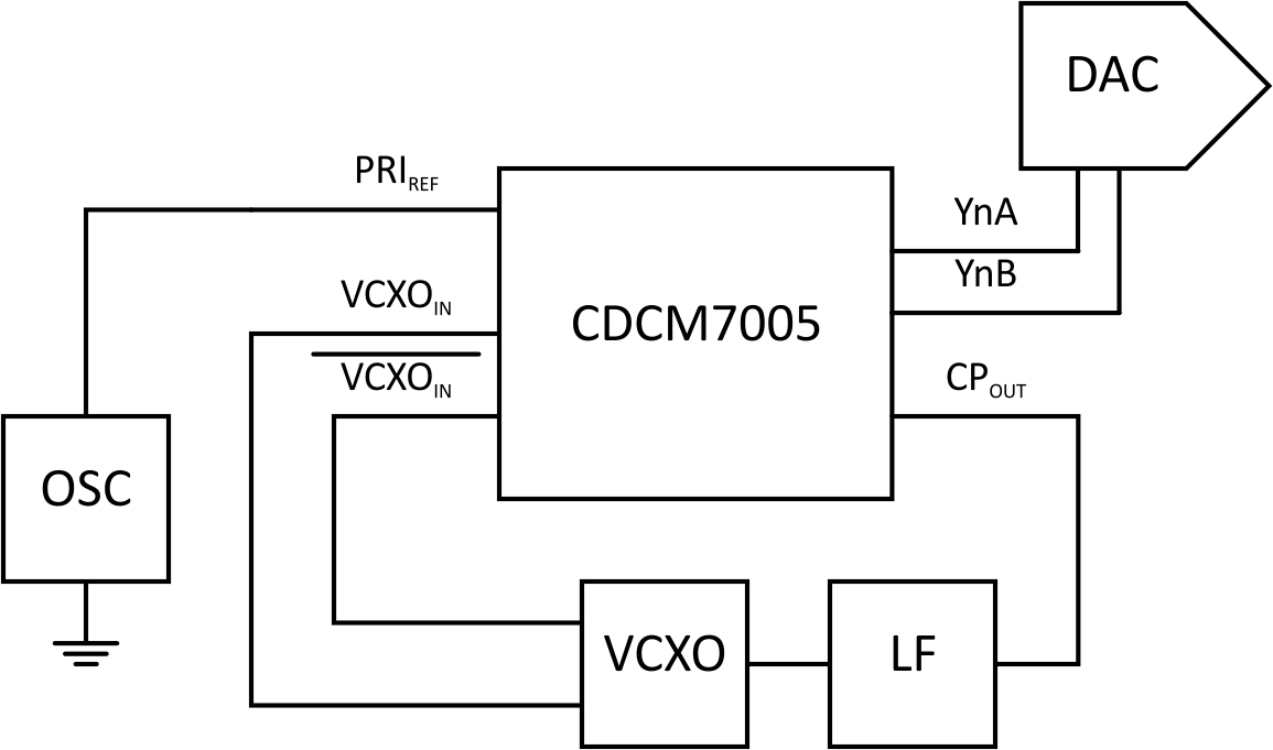
The CDCM7005 is a high-performance, low phase noise and low skew clock synchronizer that synchronizes a VCXO (voltage controlled crystal oscillator) or VCO (voltage controlled oscillator) frequency to one of the two reference clocks. The programmable pre-divider M and the feedback-dividers N and P give a high flexibility to the frequency ratio of the reference clock to VC(X)O
VC(X)O_IN clock operates up to 2.2 GHz. Through the selection of external VC(X)O and loop filter components, the PLL loop bandwidth and damping factor can be adjust to meet different system requirements.
The CDCM7005 can lock to one of two reference clock inputs (PRI_REF and SEC_REF), supports frequency hold-over mode and fast-frequency-locking for fail-safe and increased system redundancy. The outputs of the CDCM7005 are user definable and can be any combination of up to five LVPECL outputs or up to 10 LVCMOS outputs. The built in synchronization latches ensure that all outputs are synchronized for low output skew.
| PART NUMBER | PACKAGE | BODY SIZE (NOM) |
|---|---|---|
| CDCM7005 | VQFN (48) | 7.00 mm × 7.00 mm |
| BGA (64) | 8.00 mm × 8.00 mm |
- CD4016B-MIL - CMOS 四路双向开关
- ADS5271 - 具有串行化 LVDS 接口的 8 通道、12 位、40/50MSPS 的 ADC
- BQ24031 - Single-Chip Charge and System Power-Path Management IC (bqTINY-III)
- TS3DS26227 - 具有输入逻辑转换的高带宽双 SPDT 差动信号开关
- LMH0044 - SMPTE 292M / 259M 自适应电缆均衡器
- TPS61072 - Adjustable, 600-mA Switch, 90% Efficient PFM/PWM Boost Converter in ThinSOT-23
- TS3A5223 - 0.5Ω 双 SPDT 双向模拟开关
- LM3528 - 具有 128 指数明暗调节步进的高效、多显示 LED 驱动器
- CDCLVP2106 - 低抖动双路 1:6 通用 LVPECL 缓冲器
- PCM1865 - 具有智能前端的 SW 控制、4 通道音频 ADC

