



- ADS1250U - 集成电路(IC) > 数据采集 > 模数转换器(ADC)
- LM4040DIM3-10.0/NOPB - 集成电路(IC) > 电源管理(PMIC) > 电压基准
- ADS1281IPW - 集成电路(IC) > 数据采集 > 模数转换器(ADC)
- SN10502D - 集成电路(IC) > 线性 > 放大器 > 视频放大器和模块
- LP5952LC-1.5/NOPB - 集成电路(IC) > 电源管理(PMIC) > 稳压器 - 线性
- 100163DC - 集成电路(IC) > 逻辑 > 信号开关,多路复用器,解码器
- UCC21732DW - 隔离器 > 隔离器 - 栅极驱动器
- TLV62084DSGT - 集成电路(IC) > 电源管理(PMIC) > 稳压器 - DC-DC 开关稳压器
- AMC1200TDWVRQ1 - 集成电路(IC) > 线性 > 放大器 > 仪器,运算放大器,缓冲器
- CSD18513Q5A - 分立半导体产品 > 晶体管 > FET,MOSFET > 单 FET,MOSFET
- SN74BCT623DWRE4 - 逻辑 - 缓冲器,驱动器,接收器,收发器
- M0G3518QRGZRQ1 - 集成电路(IC) > 嵌入式 > 微控制器
- LMV358AQDRQ1 - 集成电路(IC) > 线性 > 放大器 > 仪器,运算放大器,缓冲器
- ADS5422Y/250 - 集成电路(IC) > 数据采集 > 模数转换器(ADC)
- TL7702ACP - 集成电路(IC) > 电源管理(PMIC) > 监控器
- INA126PA - 集成电路(IC) > 线性 > 放大器 > 仪器,运算放大器,缓冲器
- THS4130IDGKG4 - 线性器件 - 放大器 - 仪器、运算放大器、缓冲放大器
- CDCE949QPWRQ1 - 集成电路(IC) > 时钟/定时 > 时钟发生器,PLL,频率合成器
- SN74F657DWR - 集成电路(IC) > 逻辑 > 缓冲器,驱动器,接收器,收发器
- SN74AHCT574RKSR - 集成电路(IC) > 逻辑 > 触发器



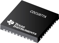
CDCU877A - 用于 DDR2 SDRAM 应用领域的 1.8V 锁相环时钟驱动器
CDCU877A是TI德州仪器公司的一款DDR2PLL产品,CDCU877A是用于 DDR2 SDRAM 应用领域的 1.8V 锁相环时钟驱动器,本站介绍了CDCU877A的封装应用图解、特点和优点、功能等,并给出了与CDCU877A相关的TI元器件型号供参考。
CDCU877A - 用于 DDR2 SDRAM 应用领域的 1.8V 锁相环时钟驱动器 - DDR2PLL - 存储器接口时钟和寄存器 - 德州仪器
The CDCU877 is a high-performance, low-jitter, low-skew, zero-delay buffer that distributes a differential clock inputpair (CK, CK) to ten differential pairs of clock outputs (Yn, Yn) and to one differential pair of feedback clock outputs (FBOUT, FBOUT). The clock outputs are controlled by the input clocks (CK, CK), the feedback clocks (FBIN, FBIN), the LVCMOS control pins (OE, OS), and the analog power input (AVDD). When OE is low, the clock outputs, except FBOUT/FBOUT, are disabled while the internal PLL continues to maintain its locked-in frequency. OS (output select) is a program pin that must be tied to GND or VDD. When OS is high, OE functions as previously described. When OS and OE are both low, OE has no affect on Y7/Y7, they are free running. When AVDD is grounded, the PLL is turned off and bypassed for test purposes.
When both clock inputs (CK, CK) are logic low, the device enters in a low power mode. An input logic detection circuit on the differential inputs, independent from input buffers, detects the logic low level and performs in a low power state where all outputs, the feedback, and the PLL are off. When the clock inputs transition from being logic low to being differential signals, the PLL turns back on, the inputs and the outputs are enabled, and the PLL obtains phase lock between the feedback clock pair (FBIN, FBIN) and the clock input pair (CK, CK) within the specified stabilization time.
The CDCU877 is able to track spread spectrum clocking (SSC) for reduced EMI. This device operates from -40°C to 85°C.
- 1.8-V Phase Lock Loop Clock Driver for Double Data Rate (DDR II) Applications
- Spread Spectrum Clock Compatible
- Operating Frequency: 10 MHz to 400 MHz
- Low Current Consumption: <135 mA
- Low Jitter (Cycle-Cycle): ±30 ps
- Low Output Skew: 35 ps
- Low Period Jitter: ±20 ps
- Low Dynamic Phase Offset: ±15 ps
- Low Static Phase Offset: ±50 ps
- Distributes One Differential Clock Input toTen Differential Outputs
- 52-Ball µBGA (MicroStar™ Junior BGA, 0,65-mm pitch) and 40-Pin MLF
- External Feedback Pins (FBIN, FBIN) are Used to Synchronize the Outputs to the Input Clocks
- Meets or Exceeds JESD82-8 PLL Standard for PC2-3200/4300
- Fail-Safe Inputs
MicroStar is a trademark of Texas Instruments.
- TPS3809L30-EP - TPS3809L30-EP, TPS3809K33-EP, TPS3809I50-EP
- TPS3619-50 - 用于 RAM 保持的电池备份监控器
- UC2845AQ - 汽车类电流模式 PWM 控制器
- MM5453 - 液晶显示驱动器(LCD 驱动器)
- LM27 - 具有固定跳变点的温度开关,120°C-150°C
- SN74LS294 - 可编程分频器/数字定时器
- 74AC11257 - 具有三态输出的四路 2 线路到 1 线路数据选择器/多路复用器
- LP5522 - 可编程 LED 驱动器
- ADC122S625 - 双路 12 位、50 kSPS 至 200 kSPS、同步采样 A/D 转换器
- LM78S40 - 通用开关稳压器子系统

