


- UCD9081RHBR - 集成电路(IC) > 电源管理(PMIC) > 监控器
- OPA1637DGKT - 集成电路(IC) > 线性 > 放大器 > 仪器,运算放大器,缓冲器
- MSP430F6765IPZ - 集成电路(IC) > 嵌入式 > 微控制器
- LM2940IMP-12/NOPB - 集成电路(IC) > 电源管理(PMIC) > 稳压器 - 线性
- TCAN330GDCNT - 集成电路(IC) > 接口 > 驱动器,接收器,收发器
- SN74AHCT573RKSR - 集成电路(IC) > 逻辑 > 锁存器
- UC2707DW - 集成电路(IC) > 电源管理(PMIC) > 栅极驱动器
- TS5L100D - 集成电路(IC) > 接口 > 模拟开关 - 特殊用途
- LP3985ITL-2.8/NOPB - 集成电路(IC) > 电源管理(PMIC) > 稳压器 - 线性
- LM9076BMA-3.3/NOPB - 集成电路(IC) > 电源管理(PMIC) > 稳压器 - 线性
- UCC27523DGNR - 集成电路(IC) > 电源管理(PMIC) > 栅极驱动器
- CD74ACT02EE4 - 集成电路(IC) > 逻辑 > 门和反相器
- LM2651EVAL - 开发板,套件,编程器 > 评估板 > DC/DC 和 AC/DC(离线)SMPS 评估板
- TL2844BDR-8 - 集成电路(IC) > 电源管理(PMIC) > DC-DC 开关控制器
- LM2577T-ADJ/LB02 - 集成电路(IC) > 电源管理(PMIC) > 稳压器 - DC-DC 开关稳压器
- ADS8863IDRCR - 集成电路(IC) > 数据采集 > 模数转换器(ADC)
- SN74LVTH373NS - 集成电路(IC) > 逻辑 > 锁存器
- ADS6224EVM - 评估板 - 模数转换器(ADC)
- SN74CBT3245CPWR - 集成电路(IC) > 逻辑 > 信号开关,多路复用器,解码器
- TRS3318IDBRG4 - 集成电路(IC) > 接口 > 驱动器,接收器,收发器


CDCVF2310 - 常规应用的高性能 1:10 时钟缓冲器
CDCVF2310是TI德州仪器公司的一款单端产品,CDCVF2310是常规应用的高性能 1:10 时钟缓冲器,本站介绍了CDCVF2310的封装应用图解、特点和优点、功能等,并给出了与CDCVF2310相关的TI元器件型号供参考。
CDCVF2310 - 常规应用的高性能 1:10 时钟缓冲器 - 单端 - 时钟缓冲器 - 德州仪器
- High-Performance 1:10 Clock Driver
- Operates up to 200MHz at VDD 3.3 V
- Pin-to-Pin Skew < 100 ps at VDD 3.3 V
- VDD Range: 2.3 V to 3.6 V
- Operating Temperature Range –40°C to 105°C
- Supports 105ºC Ambient Temperature (see Thermal Considerations)
- Output Enable Glitch Suppression
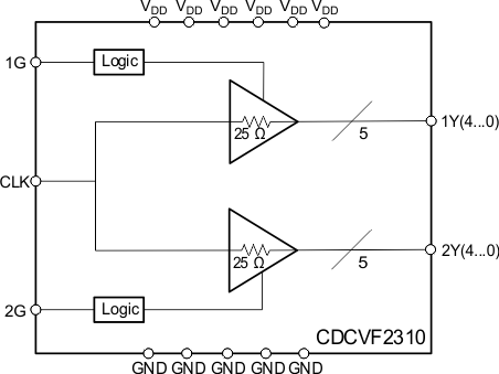
- Distributes One Clock Input to Two Banks of Five Outputs
- 25-Ω On-Chip Series Damping Resistors
- Packaged in 24-Pin TSSOP
- General-Purpose Applications
The CDCVF2310 device is a high-performance, low-skew clock buffer that operates up to 200 MHz. Two banks of five outputs each provide low-skew copies of CLK. After power up, the default state of the outputs is low regardless of the state of the control pins. For normal operation, the outputs of bank 1Y[0:4] or 2Y[0:4] can be placed in a low state when the control pins (1G or 2G, respectively) are held low and a negative clock edge is detected on the CLK input. The outputs of bank 1Y[0:4] or 2Y[0:4] can be switched into the buffer mode when the control pins (1G and 2G) are held high and a negative clock edge is detected on the CLK input. The device operates in a 2.5-V and 3.3-V environment. The built-in output enable glitch suppression ensures a synchronized output enable sequence to distribute full period clock signals.
The CDCVF2310 is characterized for operation from –40°C to 85°C.
| PART NUMBER | PACKAGE | BODY SIZE (NOM) |
|---|---|---|
| CDCVF2310 | TSSOP (24) | 4.40 mm × 7.80 mm |
- TPA6205A1 - 具有 1.8V 兼容关断电压的 1.25W 单声道全差动 AB 类音频放大器 (TPA6205)
- SN74AS02 - 四路 2 输入正或非门
- REF1933 - 双输出 Vref 和 Vref/2 电压参考
- UCC2305-Q1 - 汽车类 HID 灯控制器
- SN74AHC16374 - 具有三态输出的 16 位边沿 D 类触发器
- ADS4128 - 12 位 200MSPS 超低功耗 ADC
- CD74HC4017 - 具有 10 个解码输出的高速 CMOS 逻辑十进制计数器/除法器
- SN65LVDS324 - 高清图像传感器接收器
- OMAP3515 - 应用处理器
- TPS71812-33 - 采用 2mm x 2mm SON 封装的 200mA 输出、低噪声、高 PSRR、低压降双路稳压器

