


- SN65LVDS33DG4 - 集成电路(IC) > 接口 > 驱动器,接收器,收发器
- SN74LVC14AQPWRG4Q1 - 集成电路(IC) > 逻辑 > 门和反相器
- SN74BCT126ADRG4 - 逻辑 - 缓冲器,驱动器,接收器,收发器
- OMAPL137AZKB3 - 集成电路(IC) > 嵌入式 > 微处理器
- LMV821DBVT - 集成电路(IC) > 线性 > 放大器 > 仪器,运算放大器,缓冲器
- TMS320VC549PGE-120 - 集成电路(IC) > 嵌入式 > DSP(数字信号处理器)
- LP3875ESX-ADJ/NOPB - 集成电路(IC) > 电源管理(PMIC) > 稳压器 - 线性
- 74CBTS16212DGVRG4 - 逻辑 - 信号开关,多路复用器,解码器
- INA233EVM - 开发板,套件,编程器 > 评估板 > 评估和演示板及套件
- SN74V225-7PAG - 集成电路(IC) > 逻辑 > FIFO 存储器
- VSP2270M - 线性 - 视频处理
- LM4674TLX - 集成电路(IC) > 线性 > 放大器 > 音频放大器
- SNJ54LS49J - 集成电路(IC) > 逻辑 > 信号开关,多路复用器,解码器
- TLV9024QPWRQ1 - 集成电路(IC) > 线性 > 比较器
- TLC075CD - 集成电路(IC) > 线性 > 放大器 > 仪器,运算放大器,缓冲器
- LMX2337TMX - 集成电路(IC) > 时钟/定时 > 时钟发生器,PLL,频率合成器
- MSP430FR6977IPZR - 集成电路(IC) > 嵌入式 > 微控制器
- SN74LVC16374ADLR - 集成电路(IC) > 逻辑 > 触发器
- CDCM7005RGZRG4 - 集成电路(IC) > 时钟/定时 > 时钟发生器,PLL,频率合成器
- M38510/11904BPX - 集成电路(IC) > 线性 > 放大器 > 仪器,运算放大器,缓冲器


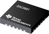
DAC9881 - 单通道 18 位低噪声电压输出数模转换器
DAC9881是TI德州仪器公司的一款精密DAC(=<10MSPS)产品,DAC9881是单通道 18 位低噪声电压输出数模转换器,本站介绍了DAC9881的封装应用图解、特点和优点、功能等,并给出了与DAC9881相关的TI元器件型号供参考。
DAC9881 - 单通道 18 位低噪声电压输出数模转换器 - 精密DAC(=<10MSPS) - 数模转换器 - 德州仪器
The DAC9881 is an 18-bit, single-channel, voltage-output digital-to-analog converter (DAC). It features 18-bit monotonicity, excellent linearity, very low-noise, and fast settling time. The on-chip precision output amplifier allows rail-to-rail output swing to be achieved over the full supply range of 2.7V to 5.5V.
The device supports a standard SPI serial interface capable of operating with input data clock frequencies up to 50MHz. The DAC9881 requires an external reference voltage to set the output range of the DAC channel. A programmable power-on reset circuit is also incorporated into the device to ensure that the DAC output powers up at zero-scale or midscale, and remains there until a valid write command.
Additionally, the DAC9881 has the capability to function in either unipolar straight binary or twos complement mode. The DAC9881 provides low-power operation. To further save energy, power-down mode can be achieved by accessing the PDN pin, thereby reducing the current consumption to 25µA at 5V. Power consumption is 4mW at 5V, reducing to 125µW in power-down mode.
The DAC9881 is available in a 4mm × 4mm QFN-24 package with a specified temperature range of -40°C to +105°C.
- 18-Bit Monotonic Over Temperature Range
- Relative Accuracy: ±2LSB Max
- Low-Noise: 24nV/Hz
- Fast Settling: 5µs
- On-Chip Output Buffer Amplifier with Rail-to-Rail Operation
- Single Power Supply: +2.7V to +5.5V
- DAC Loading Control
- Selectable Power-On Reset to Zero-Scale or Midscale
- Power-Down Mode
- Unipolar Straight Binary or Twos Complement Input Mode
- Fast SPI Interface with Schmitt-Triggered Inputs: up to 50MHz, 1.8V/3V/5V Logic
- Small Package: QFN-24, 4mm × 4mm
- APPLICATIONS
- Automatic Test Equipment
- Precision Instrumentation
- Industrial Control
- Data Acquisition Systems
All trademarks are the property of their respective owners
- BQ76920 - bqMAXIMO: μC-Controlled AFE Family for 5/10/15-Series Cell Li-Ion and Phosphate
- SN74CBT16209A - 18 位 FET 总线交换开关
- CD74AC109 - 具有设置和复位功能的双路上升沿 J-K 触发器
- ADS1293 - 用于 ECG 应用的完整低功耗集成模拟前端
- TSB81BA3E - IEEE P1394b 三端口电缆收发器/仲裁器
- DS50EV401 - 2.5 Gbps / 5.0 Gbps 或 8.0 Gbps 四路电缆和背板均衡器
- ADS8353 - 双路、700kSPS、16 位、同步采样 ADC
- SN74AUP3G14 - 低功耗三路施密特触发反向器
- MSP430FR2533 - MSP430FR263x 和 MSP430FR253x 混合信号微控制器
- SN74LS10 - 三路 3 输入正与非门

