


- LM2927T - 集成电路(IC) > 电源管理(PMIC) > 稳压器 - 线性
- CD74HCU04M96 - 集成电路(IC) > 逻辑 > 门和反相器
- TMS320DM8166SCYG - 嵌入式 - DSP(数字信号处理器)
- SN74HCS10QPWRQ1 - 集成电路(IC) > 逻辑 > 门和反相器
- SN74LVC861ADBR - 集成电路(IC) > 逻辑 > 缓冲器,驱动器,接收器,收发器
- INA600AIDBVR - 集成电路(IC) > 线性 > 放大器 > 仪器,运算放大器,缓冲器
- SN74AC573DWG4 - 集成电路(IC) > 逻辑 > 锁存器
- SN74AHC165QPWRQ1 - 集成电路(IC) > 逻辑 > 移位寄存器
- SN75LBC182DG4 - 集成电路(IC) > 接口 > 驱动器,接收器,收发器
- TPS2049DR - 集成电路(IC) > 电源管理(PMIC) > 配电开关,负载驱动器
- LM4140CCM-2.0 - 集成电路(IC) > 电源管理(PMIC) > 电压基准
- SN65HVD82DR - 集成电路(IC) > 接口 > 驱动器,接收器,收发器
- DAC8734SRHAT - 集成电路(IC) > 数据采集 > 数模转换器(DAC)
- SN74ALS561ANS - 集成电路(IC) > 逻辑 > 计数器,除法器
- LMV110M5X - 集成电路(IC) > 线性 > 放大器 > 仪器,运算放大器,缓冲器
- SN74CBT6800ADGVR - 集成电路(IC) > 逻辑 > 信号开关,多路复用器,解码器
- SN65LVCP23PWR - 集成电路(IC) > 逻辑 > 信号开关,多路复用器,解码器
- SN74F244DBR - 集成电路(IC) > 逻辑 > 缓冲器,驱动器,接收器,收发器
- SNJ54F20FK - 集成电路(IC) > 逻辑 > 门和反相器
- CD4019BE - 集成电路(IC) > 逻辑 > 门和反相器 - 多功能,可配置
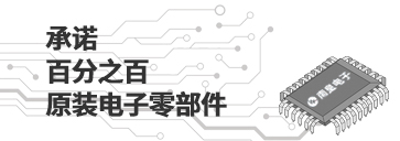


DS99R421-Q1 - 5-43 MHz FPD 链接 LVDS(3 数据 + 1 时钟)至 FPD 链接 II LVDS(嵌入式时钟 DC 平衡)转换器
DS99R421-Q1是TI德州仪器公司的一款FPD-LinkII串行器/解串器产品,DS99R421-Q1是5-43 MHz FPD 链接 LVDS(3 数据 + 1 时钟)至 FPD 链接 II LVDS(嵌入式时钟 DC 平衡)转换器,本站介绍了DS99R421-Q1的封装应用图解、特点和优点、功能等,并给出了与DS99R421-Q1相关的TI元器件型号供参考。
DS99R421-Q1 - 5-43 MHz FPD 链接 LVDS(3 数据 + 1 时钟)至 FPD 链接 II LVDS(嵌入式时钟 DC 平衡)转换器 - FPD-LinkII串行器/解串器 - 显示和成像串行器/解串器 - 德州仪器
The DS99R421 converts a FPD-Link input with 4 non-DC Balanced LVDS (3 LVDS Data + LVDS Clock) plus 3 over-sampled low speed control bits into a single LVDS DC-balanced serial stream with embedded clock information. This single serial stream simplifies transferring the 24-bit bus over a single differential pair of PCB traces and cable by eliminating the skew problems between the 3 parallel LVDS data inputs and LVDS clock paths. It saves system cost by narrowing 4 LVDS pairs to 1 LVDS pair that in turn reduce PCB layers, cable width, connector size, and pins.
The DS99R421 incorporates a single serialized LVDS signal on the high-speed I/O. Embedded clock LVDS provides a low power and low noise environment for reliably transferring data over a serial transmission path. By optimizing the converter output edge rate for the operating frequency range EMI is further reduced.
In addition the device features pre-emphasis to boost signals over longer distances using lossy cables. Internal DC balanced encoding is used to support AC-Coupled interconnects.
- 5 MHz–43 MHz Embedded Clock & DC-Balanced Data Transmission (21 Total LVDS Data Bits Plus 3 Low Speed LVCMOS Data Bits)
- User Adjustable Pre-Emphasis Driving Ability Through External Resistor on LVDS Outputs and Capable to Drive up to 10 Meters Shielded Twisted-Pair Cable
- Supports AC-Coupling Data Transmission
- 100? Integrated Termination Resistor at LVDS Input
- Power-Down Control
- Available @SPEED BIST to DS90UR124 to Validate Link Integrity
- All LVCMOS Inputs & Control Pins Have Internal Pulldown
- Schmitt Trigger Inputs on OS[2:0] to Minimize Metastable Conditions
- Outputs Tri-Stated Through DEN
- On-Chip Filters for PLLs
- Power Supply Range 3.3V ± 10%
- Automotive Temperature Range −40°C to +105°C
- Greater Than 8kV ESD Tolerance
- Meets ISO 10605 ESD and AEC-Q100 Compliance
- UC2854BM - 增强型高功率因子前置稳压器
- TPS92315 - 离线初级测感应控制器
- TPS2828 - 反向高速 MOSFET 驱动器
- LM20146 - 6A,可调节频率同步降压稳压器
- SN74CB3Q3305 - 双路 FET 2.5V/3.3V 低电压高带宽总线开关
- TPS25921A - 具有精密限流功能的 4.5V-18V 熔丝
- SN65HVD30-EP - SN65HVD30-EP, SN65HVD39-EP
- DS90UB903Q-Q1 - 具有双向控制通道的 10 - 43MHz 18 位色彩 FPD 链接 III 串行器
- SN55LBC175 - 四路低功耗差动线路接收器
- HD3SS6126 - USB 3.0 差动开关 2:1/1:2 MUX/DEMUX

