


- TRS3223QPWRQ1 - 集成电路(IC) > 接口 > 驱动器,接收器,收发器
- SN74ALS29825DW - 集成电路(IC) > 逻辑 > 缓冲器,驱动器,接收器,收发器
- DAC5578SPWR - 集成电路(IC) > 数据采集 > 数模转换器(DAC)
- LM95010CIMM - 传感器,变送器 > 温度传感器 > 模拟和数字输出
- SN74AHC02PWR - 集成电路(IC) > 逻辑 > 门和反相器
- LM4132CQ1MFT3.0 - 集成电路(IC) > 电源管理(PMIC) > 电压基准
- LM4040CIM3-2.5 - 集成电路(IC) > 电源管理(PMIC) > 电压基准
- SN74F161ANG4 - 集成电路(IC) > 逻辑 > 计数器,除法器
- MSC1210Y3PAGT - 集成电路(IC) > 数据采集 > ADC/DAC - 特殊用途
- LM3S818-IQN50-C2 - 集成电路(IC) > 嵌入式 > 微控制器
- TLV62585PEVM-030 - 开发板,套件,编程器 > 评估板 > DC/DC 和 AC/DC(离线)SMPS 评估板
- TMS320F28374DZWTT - 集成电路(IC) > 嵌入式 > 微控制器
- ADS7826IDRBTG4 - 集成电路(IC) > 数据采集 > 模数转换器(ADC)
- TPS2421-1DDA - 集成电路(IC) > 电源管理(PMIC) > 热插拔控制器
- TL4051A12IDBZRG4 - 集成电路(IC) > 电源管理(PMIC) > 电压基准
- TPS75333QPWPR - 集成电路(IC) > 电源管理(PMIC) > 稳压器 - 线性
- SN74AS641DWR - 集成电路(IC) > 逻辑 > 缓冲器,驱动器,接收器,收发器
- THS4503CDR - 集成电路(IC) > 线性 > 放大器 > 仪器,运算放大器,缓冲器
- F28P650DK8NMRR - 集成电路(IC) > 嵌入式 > 微控制器
- TPS3850G30QDRCRQ1 - 集成电路(IC) > 电源管理(PMIC) > 监控器


RM48L530 - 16/32-Bit RISC Flash Microcontroller
RM48L530是TI德州仪器公司的一款安全产品,RM48L530是16/32-Bit RISC Flash Microcontroller,本站介绍了RM48L530的封装应用图解、特点和优点、功能等,并给出了与RM48L530相关的TI元器件型号供参考。
RM48L530 - 16/32-Bit RISC Flash Microcontroller - 安全 - 高性能MCU - 德州仪器
- High-Performance Microcontroller for Safety-Critical Applications
- Dual CPUs Running in Lockstep
- ECC on Flash and RAM Interfaces
- Built-In Self-Test (BIST) for CPU and On-chip RAMs
- Error Signaling Module With Error Pin
- Voltage and Clock Monitoring
- ARM®Cortex®-R4F 32-Bit RISC CPU
- Efficient 1.66 DMIPS/MHz With 8-Stage Pipeline
- FPU With Single- and Double-Precision
- 12-Region Memory Protection Unit (MPU)
- Open Architecture With Third-Party Support
- Operating Conditions
- System Clock up to 200 MHz
- Core Supply Voltage (VCC): 1.2 V Nominal
- I/O Supply Voltage (VCCIO): 3.3 V Nominal
- ADC Supply Voltage (VCCAD): 3.0 to 5.25 V
- Integrated Memory
- 3MB of Program Flash With ECC (RM48L930)
- 2MB of Program Flash With ECC (RM48L730/530)
- 256KB of RAM With ECC (RM48L930/730)
- 192KB of RAM With ECC (RM48L530)
- 64KB of Flash With ECC for Emulated EEPROM
- 16-Bit External Memory Interface
- Common Platform Architecture
- Consistent Memory Map Across Family
- Real-Time Interrupt (RTI) Timer OS Timer
- 96-Channel Vectored Interrupt Module (VIM)
- 2-Channel Cyclic Redundancy Checker (CRC)
- Direct Memory Access (DMA) Controller
- 16 Channels and 32 Peripheral Requests
- Parity Protection for Control Packet RAM
- DMA Accesses Protected by Dedicated MPU
- Frequency-Modulated Phase-Locked Loop (FMPLL) With Built-In Slip Detector
- Separate Nonmodulating PLL
- Trace and Calibration Capabilities
- Embedded Trace Macrocell (ETM-R4)
- Data Modification Module (DMM)
- RAM Trace Port (RTP)
- Parameter Overlay Module (POM)
- Multiple Communication Interfaces
- USB
- 2-Port USB Host Controller
- One Full-Speed USB Device Port
- Three CAN Controllers (DCANs)
- 64 Mailboxes, Each With Parity Protection
- Compliant to CAN Protocol Version 2.0B
- Standard Serial Communication Interface (SCI)
- Local Interconnect Network (LIN) Interface Controller
- Compliant to LIN Protocol Version 2.1
- Can be Configured as a Second SCI
- Inter-Integrated Circuit (I2C)
- Three Multibuffered Serial Peripheral Interfaces (MibSPIs)
- 128 Words With Parity Protection Each
- Two Standard Serial Peripheral Interfaces (SPIs)
- USB
- Two Next Generation High-End Timer (N2HET) Modules
- N2HET1: 32 Programmable Channels
- N2HET2: 18 Programmable Channels
- 160-Word Instruction RAM Each With Parity Protection
- Each N2HET Includes Hardware Angle Generator
- Dedicated High-End Transfer Unit (HTU) With MPU for Each N2HET
- Two 12-Bit Multibuffered ADC Modules
- ADC1: 24 Channels
- ADC2: 16 Channels Shared With ADC1
- 64 Result Buffers With Parity Protection Each
- General-Purpose Input/Output (GPIO) Pins Capable of Generating Interrupts
- 16 Pins on the ZWT Package
- 10 Pins on the PGE Package
- IEEE 1149.1 JTAG, Boundary Scan and ARM CoreSight™ Components
- JTAG Security Module
- Packages
- 144-Pin Quad Flatpack (PGE) [Green]
- 337-Ball Grid Array (ZWT) [Green]
- Industrial Safety Applications
- Industrial Automation
- Safe Programmable Logic Controllers (PLCs)
- Power Generation and Distribution
- Turbines and Windmills
- Elevators and Escalators
- Medical Applications
- Ventilators
- Defibrillators
- Infusion and Insulin Pumps
- Radiation Therapy
- Robotic Surgery
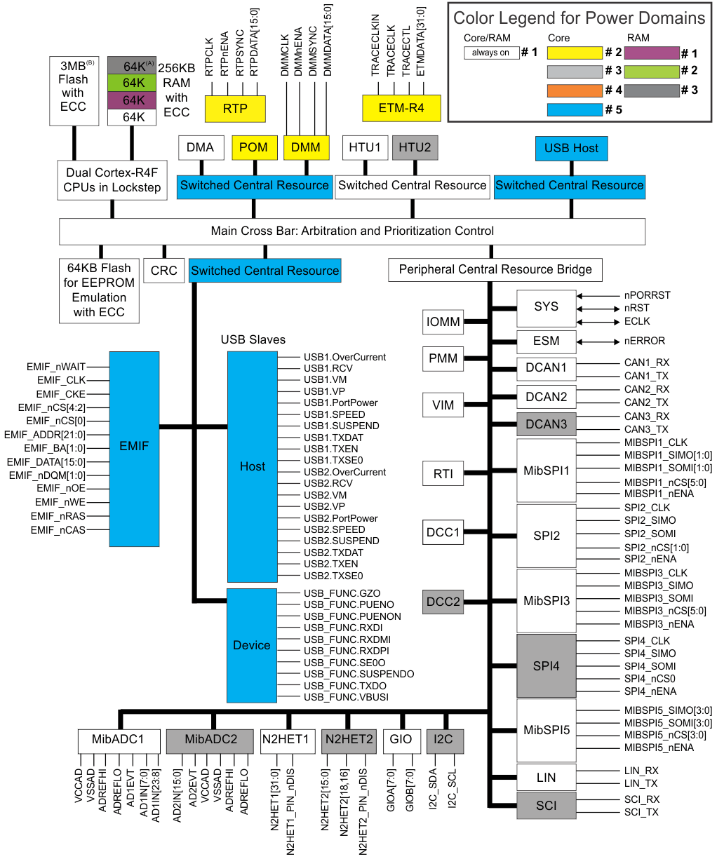
The RM48Lx30 device is a high-performance microcontroller family for safety systems. The safety architecture includes dual CPUs in lockstep, CPU and memory BIST logic, ECC on both the flash and the data SRAM, parity on peripheral memories, and loopback capability on peripheral I/Os.
The RM48Lx30 device integrates the ARM Cortex-R4F Floating-Point CPU. The CPU offers an efficient 1.66 DMIPS/MHz, and has configurations that can run up to 200 MHz, providing up to 332 DMIPS. The device supports the little-endian [LE] format.
The RM48L930 device has 3MB of integrated flash and 256KB of data RAM. The RM48L730 has 2MB of integrated flash and 256KB of data RAM. The RM48L530 device has 2MB of integrated flash and 192KB of data RAM. Both the flash and RAM have single-bit error correction and double-bit error detection. The flash memory on this device is a nonvolatile, electrically erasable, and programmable memory implemented with a 64-bit-wide data bus interface. The flash operates on a 3.3-V supply input (same level as I/O supply) for all read, program, and erase operations. When in pipeline mode, the flash operates with a system clock frequency of up to 200 MHz. The SRAM supports single-cycle read and write accesses in byte, halfword, word, and double-word modes.
The RM48Lx30 device features peripherals for real-time control-based applications, including two Next Generation High-End Timer (N2HET) timing coprocessors and two 12-bit Analog-to-Digital Converters (ADCs) supporting up to 24 inputs.
The N2HET is an advanced intelligent timer that provides sophisticated timing functions for real-time applications. The timer is software-controlled, using a reduced instruction set, with a specialized timer micromachine and an attached I/O port. The N2HET can be used for pulse-width-modulated outputs, capture or compare inputs, or GPIO. The N2HET is especially well suited for applications requiring multiple sensor information and drive actuators with complex and accurate time pulses. A High-End Timer Transfer Unit (HTU) can perform DMA-type transactions to transfer N2HET data to or from main memory. A Memory Protection Unit (MPU) is built into the HTU.
The device has two 12-bit-resolution MibADCs with 24 channels and 64 words of parity-protected buffer RAM each. The MibADC channels can be converted individually or can be grouped by software for sequential conversion sequences. Sixteen channels are shared between the two MibADCs. There are three separate groupings. Each sequence can be converted once when triggered or configured for continuous conversion mode. The MibADC has a 10-bit mode for use when compatibility with older devices or faster conversion time is desired.
The device has multiple communication interfaces: three MibSPIs, two SPIs, one LIN, one SCI, three DCANs, and one I2C module. The SPIs provide a convenient method of serial high-speed communication between similar shift-register type devices. The LIN supports the Local Interconnect standard 2.0 and can be used as a UART in full-duplex mode using the standard Non-Return-to-Zero (NRZ) format.
The DCAN supports the CAN 2.0 (A and B) protocol standard and uses a serial, multimaster communication protocol that efficiently supports distributed real-time control with robust communication rates of up to 1 Mbps. The DCAN is ideal for systems operating in noisy and harsh environments (for example, automotive vehicle networking and industrial fieldbus) that require reliable serial communication or multiplexed wiring.
The I2C module is a multimaster communication module providing an interface between the microcontroller and an I2C-compatible device through the I2C serial bus. The I2C supports speeds of 100 and 400 Kbps.
The Frequency-Modulated Phase-Locked Loop (FMPLL) clock module is used to multiply the external frequency reference to a higher frequency for internal use. There are two FMPLL modules on this device. These modules, when enabled, provide two of the seven possible clock source inputs to the Global Clock Module (GCM). The GCM manages the mapping between the available clock sources and the device clock domains.
The device also has an External Clock Prescaler (ECP) module that when enabled, outputs a continuous external clock on the ECLK pin (or ball). The ECLK frequency is a user-programmable ratio of the peripheral interface clock (VCLK) frequency. This low-frequency output can be monitored externally as an indicator of the device operating frequency.
The DMA controller has 16 channels, 32 peripheral requests, and parity protection on its memory. An MPU is built into the DMA to limit the DMA to prescribed areas of memory and to protect the rest of the memory system from any malfunction of the DMA.
The Error Signaling Module (ESM) monitors all device errors and determines whether an interrupt is generated or the external ERROR pin is toggled when a fault is detected. The ERROR pin can be monitored externally as an indicator of a fault condition in the microcontroller.
The External Memory Interface (EMIF) provides off-chip expansion capability with the ability to interface to synchronous DRAM (SDRAM) devices, asynchronous memories, peripherals, or FPGA devices.
Several interfaces are implemented to enhance the debugging capabilities of application code. In addition to the built-in ARM Cortex-R4F CoreSight debug features, an External Trace Macrocell (ETM) provides instruction and data trace of program execution. For instrumentation purposes, a RAM Trace Port (RTP) module is implemented to support high-speed tracing of RAM and peripheral accesses by the CPU or any other master. A Data Modification Module (DMM) gives the ability to write external data into the device memory. Both the RTP and DMM have no or only minimum impact on the program execution time of the application code. A Parameter Overlay Module (POM) can reroute flash accesses to internal memory or to the EMIF. This rerouting allows the dynamic calibration against production code of parameters and tables without rebuilding the code to explicitly access RAM or halting the processor to reprogram the data flash.
With integrated safety features and a wide choice of communication and control peripherals, the RM48Lx30 device is an ideal solution for high-performance real-time control applications with safety-critical requirements.
| PART NUMBER | PACKAGE | BODY SIZE |
|---|---|---|
| RM48L930ZWT | NFBGA (337) | 16.0 mm × 16.0 mm |
| RM48L930PGE | LQFP (144) | 20.0 mm × 20.0 mm |
| RM48L730ZWT | NFBGA (337) | 16.0 mm × 16.0 mm |
| RM48L730PGE | LQFP (144) | 20.0 mm × 20.0 mm |
| RM48L530ZWT | NFBGA (337) | 16.0 mm × 16.0 mm |
| RM48L530PGE | LQFP (144) | 20.0 mm × 20.0 mm |
- CD4031B-MIL - CMOS 64 级静态移位寄存器
- MSP430F6777A - MSP430F677xA、MSP430F676xA 、MSP430F674xA 混合信号微控制器
- LM1771 - 具有精密启用和无需外部补偿组件的低压同步降压控制器
- CD74AC10 - 三路 3 输入与非门
- TPS65161 - 4 通道 LCD 偏置(2.8A 最低 升压 Ilim. 高达 19V,2.3A 最低 降压 Ilim)
- CDC391 - 具有可选择极性的 1 至 6 时钟驱动器
- HD3SS3415 - 4 通道高性能 10Gbps 差动开关
- CD74HC154 - 高速 CMOS 逻辑 4 至 16 线路解码器/多路解复用器
- SN54ALS580B - 具有三态输出的八路 D 类透明锁存器
- SN74ABTH32501 - 具有三态输出的 36 位通用总线收发器

