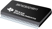

SN74CB3Q16811是TI公司的一款数字开关产品,SN74CB3Q16811是具有预充电输出的 24 位 FET 开关,2.5V/3.3V 低压高带宽总线开关,本页介绍了SN74CB3Q16811的产品说明、应用、特性等,并给出了与SN74CB3Q16811相关的TI元器件型号供参考。
SN74CB3Q16811 - 具有预充电输出的 24 位 FET 开关,2.5V/3.3V 低压高带宽总线开关 - 数字开关 - 信号开关 - TI公司(Texas Instruments,德州仪器)
The SN74CB3Q16811 is a high-bandwidth FET bus switch utilizing a charge pump to elevate the gate voltage of the pass transistor, providing a low and flat ON-state resistance (ron). The low and flat ON-state resistance allows for minimal propagation delay and supports rail-to-rail switching on the data input/output (I/O) ports. The device also features low data I/O capacitance to minimize capacitive loading and signal distortion on the data bus. Specifically designed to support high-bandwidth applications, the SN74CB3Q16811 provides an optimized interface solution ideally suited for broadband communications, networking, and data-intensive computing systems.
The SN74CB3Q16811 is organized as two 12-bit bus switches with separate output-enable (1OE\, 2OE\) inputs. It can be used as two 12-bit bus switches or as one 24-bit bus switch. When OE\ is low, the associated 12-bit bus switch is ON, and the A port is connected to the B port, allowing bidirectional data flow between ports. When OE is high, the associated 12-bit bus switch is OFF, and a high-impedance state exists between the A and B ports. The B port is precharged to BIASV through the equivalent of a 10-k resistor when OE\ is high, or if the device is powered down (VCC = 0 V).
During insertion (or removal) of a card into (or from) an active bus, the card’s output voltage may be close to GND. When the connector pins make contact, the card’s parasitic capacitance tries to force the bus signal to GND, creating a possible glitch on the active bus. This glitching effect can be reduced by using a bus switch with precharged bias voltage (BIASV) of the bus switch equal to the input threshold voltage level of the receivers on the active bus. This method will ensure that any glitch produced by insertion (or removal) of the card will not cross the input threshold region of the receivers on the active bus, minimizing the effects of live-insertion noise.
This device is fully specified for partial-power-down applications using Ioff. The Ioff circuitry prevents damaging current backflow through the device when it is powered down.
To ensure the high-impedance state during power up or power down, OE\ should be tied to VCC through a pullup resistor; the minimum value of the resistor is determined by the current-sinking capability of the driver.
- Member of the Texas Instruments Widebus™ Family
- SN74CB3Q Bus Switches Are Equivalent to IDTQS3VH Bus Switches
- 5-V-Tolerant I/Os with Device Powered-Up or Powered-Down
- Low and Flat ON-State Resistance (ron) Characteristics Over Operating Range
- Rail-to-Rail Switching on Data I/O Ports
- 0- to 5-V Switching With 3.3-V VCC
- 0- to 3.3-V Switching With 2.5-V VCC
- B-Port Outputs Are Precharged by Bias Voltage (BIASV) to Minimize Signal Distortion During Live Insertion and Hot-Plugging
- Supports PCI Hot Plug
- Bidirectional Data Flow, With Near-Zero Propagation Delay
- Low Input/Output Capacitance Minimizes Loading and Signal Distortion (Cio(OFF) = 4 pF Typ)
- Fast Switching Frequency (fON\ = 20 MHz Max)
- Data and Control Inputs Provide Undershoot Clamp Diodes
- Low Power Consumption (ICC = 0.75 mA Typ)
- VCC Operating Range From 2.3 V to 3.6 V
- Data I/Os Support 0 to 5-V Signaling Levels (0.8-V, 1.2-V, 1.5-V, 1.8-V, 2.5-V, 3.3-V, 5-V)
- Control Inputs Can Be Driven by TTL or 5-V/3.3-V CMOS Outputs
- Ioff Supports Partial-Power-Down Mode Operation
- Latch-Up Performance Exceeds 100 mA Per JESD 78, Class II
- ESD Performance Tested Per JESD 22
- 2000-V Human-Body Model (A114-B, Class II)
- 1000-V Charged-Device Model (C101)
- Supports Both Digital and Analog Applications: PCI Hot Plug, Hot Docking, Memory Interleaving, Bus Isolation, Low-Distortion Signal Gating
For additional information regarding the performance characteristics of the CB3Q family, refer to the TI application report, CBT-C, CB3T, and CB3Q Signal-Switch Families, literature number SCDA008. Widebus is a trademark of Texas Instruments.


