


- THS3111EVM - 开发板,套件,编程器 > 评估板 > 运算放大器评估板
- REF02AU/2K5G4 - 集成电路(IC) > 电源管理(PMIC) > 电压基准
- TPS70615DRVT - 集成电路(IC) > 电源管理(PMIC) > 稳压器 - 线性
- TMS320C6678CYP25 - 集成电路(IC) > 嵌入式 > DSP(数字信号处理器)
- BQ296224DSGT - 集成电路(IC) > 电源管理(PMIC) > 电池管理
- SN74ALVC16721DL - 集成电路(IC) > 逻辑 > 缓冲器,驱动器,接收器,收发器
- LMV1091TM/NOPB - 集成电路(IC) > 线性 > 放大器 > 音频放大器
- TLC084IN - 集成电路(IC) > 线性 > 放大器 > 仪器,运算放大器,缓冲器
- TPS65257EVM - 开发板,套件,编程器 > 评估板 > DC/DC 和 AC/DC(离线)SMPS 评估板
- LM4040B25IDBZR - 集成电路(IC) > 电源管理(PMIC) > 电压基准
- MAX3243ECDW - 集成电路(IC) > 接口 > 驱动器,接收器,收发器
- SN74HCT139PWR - 集成电路(IC) > 逻辑 > 信号开关,多路复用器,解码器
- SN74LVT245BPWRG4 - 集成电路(IC) > 逻辑 > 缓冲器,驱动器,接收器,收发器
- DAC60501MDGST - 集成电路(IC) > 数据采集 > 数模转换器(DAC)
- OPA2822U - 集成电路(IC) > 线性 > 放大器 > 仪器,运算放大器,缓冲器
- OPT101P - 传感器,变送器 > 光学传感器 > 环境光、IR 红外线、UV 紫外线传感器
- CDCM7005RGZR - 集成电路(IC) > 时钟/定时 > 时钟发生器,PLL,频率合成器
- SN74ALVCH162601DLR - 集成电路(IC) > 逻辑 > 通用总线功能
- TPS3435CAIEGDDFR - 集成电路(IC) > 电源管理(PMIC) > 监控器
- CSD15380F3 - 分立半导体产品 > 晶体管 > FET,MOSFET > 单 FET,MOSFET
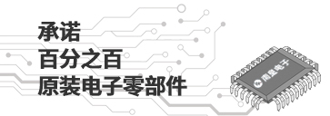


SN74LS374 - 具有三态输出的八路 D 类边沿触发器
SN74LS374是TI德州仪器公司的一款D类触发器产品,SN74LS374是具有三态输出的八路 D 类边沿触发器,本站介绍了SN74LS374的封装应用图解、特点和优点、功能等,并给出了与SN74LS374相关的TI元器件型号供参考。
SN74LS374 - 具有三态输出的八路 D 类边沿触发器 - D类触发器 - 触发器/锁存器/寄存器 - 德州仪器
These 8-bit registers feature 3-state outputs designed specifically for driving highly capacitive or relatively low-impedance loads. The high-impedance 3-state and increased high-logic-level drive provide these registers with the capability of being connected directly to and driving the bus lines in a bus-organized system without need for interface or pullup components. These devices are particularly attractive for implementing buffer registers, I/O ports, bidirectional bus drivers, and working registers.
The eight latches of the ’LS373 and ’S373 are transparent D-type latches, meaning that while the enable (C or CLK) input is high, the Q outputs follow the data (D) inputs. When C or CLK is taken low, the output is latched at the level of the data that was set up.
The eight flip-flops of the ’LS374 and ’S374 are edge-triggered D-type flip-flops. On the positive transition of the clock, the Q outputs are set to the logic states that were set up at the D inputs.
Schmitt-trigger buffered inputs at the enable/clock lines of the ’S373 and ’S374 devices simplify system design as ac and dc noise rejection is improved by typically 400 mV due to the input hysteresis. A buffered output-control (OC) input can be used to place the eight outputs in either a normal logic state (high or low logic levels) or the high-impedance state. In the high-impedance state, the outputs neither load nor drive the bus lines significantly.
OC\ does not affect the internal operation of the latches or flip-flops. That is, the old data can be retained or new data can be entered, even while the outputs are off.
- Choice of Eight Latches or Eight D-Type Flip-Flops in a Single Package
- 3-State Bus-Driving Outputs
- Full Parallel Access for Loading
- Buffered Control Inputs
- Clock-Enable Input Has Hysteresis to Improve Noise Rejection (’S373 and ’S374)
- P-N-P Inputs Reduce DC Loading on Data Lines (’S373 and ’S374)
- SN54ALS520 - 8 位等值比较器
- PTH03010W - 15A 输出 3.3V 输入的非隔离宽输出调节电源模块
- ADS8482 - 具有 Ref 引脚和伪双极全差动输入的 18 位 1MSPS 并行 ADC
- PTH03050Y - 用于 DDR/QDR 存储器的 6A 输出 3.3V 输入的总线终端电源模块
- LM3648 - LM3648 具有 1.5A 高侧电流源的同步升压 LED 闪存驱动器
- SN74LVC00A - 四路 2 输入正与非门
- MSP430G2353 - MSP430G2x53、MSP430G2x13 混合信号微处理器
- LM285-1.2 - 微功耗电压参考
- BQ51051B - 集成无线电源锂离子充电器接收器,符合 Qi (WPC) 标准
- ADS8372 - 具有 Ref 引脚和伪双极全差动输入的 16 位 600KSPS 串行 ADC

