



- OMAP3503DCBBA - 嵌入式 - 微处理器
- SN74BCT2240DBR - 逻辑 - 缓冲器,驱动器,接收器,收发器
- LM6132BIMX - 集成电路(IC) > 线性 > 放大器 > 仪器,运算放大器,缓冲器
- MSP-FET430P430 - 开发板,套件,编程器 > 编程器、仿真器和调试器
- LM3670MF-1.875 - 集成电路(IC) > 电源管理(PMIC) > 稳压器 - DC-DC 开关稳压器
- SN751730DE4 - 集成电路(IC) > 接口 > 驱动器,接收器,收发器
- SN74HCT573N - 集成电路(IC) > 逻辑 > 锁存器
- LMX2330ATMX - 集成电路(IC) > 时钟/定时 > 时钟发生器,PLL,频率合成器
- TRF4400PWR - 射频和无线 > 射频发射器
- TLC2274ACPWRG4 - 集成电路(IC) > 线性 > 放大器 > 仪器,运算放大器,缓冲器
- SN74ACT32DRG4 - 集成电路(IC) > 逻辑 > 门和反相器
- TPS62311YZDT - 集成电路(IC) > 电源管理(PMIC) > 稳压器 - DC-DC 开关稳压器
- SN74LVC1G66YEAR - 集成电路(IC) > 接口 > 模拟开关,多路复用器,解复用器
- PT4826N - 直流转换器
- TLV341IDRLR - 集成电路(IC) > 线性 > 放大器 > 仪器,运算放大器,缓冲器
- TPS54311PWPR - 集成电路(IC) > 电源管理(PMIC) > 稳压器 - DC-DC 开关稳压器
- LM2941T/LB04 - 集成电路(IC) > 电源管理(PMIC) > 稳压器 - 线性
- CD4073BM - 集成电路(IC) > 逻辑 > 门和反相器
- SN74AHCT123APWR - 集成电路(IC) > 逻辑 > 多谐振荡器
- DS90CF561MTD/NOPB - 集成电路(IC) > 接口 > 专用



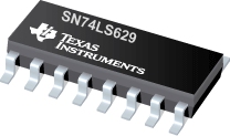
SN74LS629 - 双电压控制震荡器
SN74LS629是TI德州仪器公司的一款锁相环(PLL)/振荡器产品,SN74LS629是双电压控制震荡器,本站介绍了SN74LS629的封装应用图解、特点和优点、功能等,并给出了与SN74LS629相关的TI元器件型号供参考。
SN74LS629 - 双电压控制震荡器 - 锁相环(PLL)/振荡器 - 特殊逻辑 - 德州仪器
These voltage-controlled oscillators (VCOs) are improved versions of the original VCO family: SN54LS124, SN54LS324 thru SN54LS327, SN74LS124, and SN74LS324 thru SN74LS327. These new devices feature improved voltage-to-frequency linearity, range, and compensation. With the exception of the 'LS624 and 'LS628, all of these devices feature two independent VCOs in a single monolithic chip. The 'LS624, 'LS625, 'LS626, and 'LS628 have complementary Z outputs. The output frequency for each VCO is established by a single external component (either a capacitor or crystal) in combination with voltage-sensitive inputs used for frequency control and frequency range. Each device has a voltage-sensitive input for frequency control; however, the 'LS624, 'LS628, and 'LS629 devices also have one for frequency range. (See Figures 1 thru 6).
The 'LS628 offers more precise temperature compensation than its 'LS624 counterpart. The 'LS624 features a 600 ohm internal timing resistor. The 'LS628 requires a timing resistor to be connected externally across Rext pins. Temperature compensation will be improved due to the temperature coefficient of the external resistor.
Figure 3 and Figure 6 contain the necessary information to choose the proper capacitor value to obtain the desired operating frequency.
A single 5-volt supply can be used: however, one set of supply voltage and ground pins (VCC and GND) is provided for the enable, synchronization-gating, and output sections, and a separate set (OSC VCC and OSC GND) is provided for the oscillator and associated frequency-control circuits so that effective isolation can be accomplished in the system. For operation of frequencies greater than 10 MHz, it is recommended that two independent supplies be used. Disabling either VCO of the 'LS625 and 'LS625 and 'LS627 can be achieved by removing the appropriate OSC VCC. An enable input is provided on the 'LS624, 'LS626, 'LS628, and 'LS629. When the enable input is low, the output is enabled: when the enable input is high, the internal oscillator is disabled, Y is high, and Z is low. Caution! Crosstalk may occur in the dual devices ('LS625, 'LS626, 'LS627 and 'LS629) when both VCOs are operated simultaneously. To minimize crosstalk, either of the following are recommended: (A) If frequencies are widely separated, use a 10-μh inductor between VCC pins. (B) If frequencies are closely spaced, use two separate VCC supplies or place two series diodes between the VCC pins.
The pulse-synchronization-gating section ensures that the first output pulse is neither clipped nor extended. The duty cycle of the square-wave output is fixed at approximately 50 percent.
The SN54LS624 thru SN54LS629 are characterized for operation over the full military temperature range of -55°C to 125°C. The SN74LS624 thru SN74LS629 are characterized for operation from 0°C to 70°C.
- Separate Supply Voltage Pins for Isolation of Frequency Control Inputs and Oscillators from Output Circuitry
- Highly Stable Operation over Specified Temperature and/or Supply Voltage Ranges
- SA555 - 精密定时器
- SN74SSTU32864 - 具有 SSTL_18 输入和输出的 25 位可配置寄存缓冲器
- UC3717A - 步进电机驱动电路
- LMP91050 - 气体/化学感应
- TPS54622 - 具有断续电流限制功能的 4.5V 至 17 V 输入、6A 同步降压 SWIFT? 转换器
- LM5025C - 有源钳位电压模式 PWM 控制器
- CDC421A212 - 完全集成的固定频率低抖动晶振时钟发生器
- LM3420 - 锂离子电池充电控制器
- SN54LS684 - 8 位幅度/等值比较器
- LM97937 - 具有 SNRBoost、Bit-Burst 和 JESD204B 输出的 LM97937 双路 9 位 370MSPS ADC

