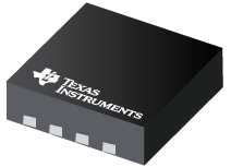

LMV112是TI公司的一款单端产品,LMV112是40 MHz 双路时钟缓冲器,本页介绍了LMV112的产品说明、应用、特性等,并给出了与LMV112相关的TI元器件型号供参考。
LMV112 - 40 MHz 双路时钟缓冲器 - 单端 - 时钟缓冲器 - TI公司(Texas Instruments,德州仪器)
The LMV112 is a high speed dual clock buffer designed for portable communications and accurate multi-clock systems. The LMV112 integrates two 40MHz low noise buffers which optimizes application and out performs large discrete solutions. This device enables superb system operation between the base band and the oscillator signal path while eliminating crosstalk.
Texas Instruments' unique technology and design deliver accuracy, capacitance and load resistance while increasing the drive capability of the device. The low power consumption makes the LMV112 perfect for battery applications.
The robust, independent, and flexible buffers are designed to provide the customer with the ability to manage complex clock signals in the latest wireless applications. The buffers deliver 110 V/μs internal slew rate with independent shutdown and duty cycle precision. The patented analog circuit drives capacitive loads beyond 20pF. Texas Instruments' proven biasing technique has 1V centering, rail-to-rail input/output unity gain, and AC coupled convenient inputs. These integrated cells save space and require no external bias resistors. Texas Instruments' rapid recovery after disable optimizes performance and current consumption. The LMV112 offers individual enable pin controls and since there is no internal ground reference either single or split supply configurations offer additional system flexibility and power choices.
The LMV112 is a proven replacement for any discrete circuitry and simplifies board layout while minimizing related parasitic components.
The LMV112 is produced in the small WSON package which offers high quality while minimizing its use of PCB space. Texas Instruments' advanced packaging offers direct PCB-IC evaluation via pin access.
- (Typical Values are: VSUPPLY = 2.7V and CL = 20pF, Unless Otherwise Specified.)
- Small Signal Bandwidth 40 MHz
- Supply Voltage Range 2.4V to 5V
- Slew Rate 110 V/μs
- Total Supply Current 1.6 mA
- Shutdown Current 59 µA
- Rail-to-Rail Input and Output
- Individual Buffer Enable Pins
- Rapid Ton Technology
- Crosstalk Rejection Circuitry
- 8-pin WSON, Pin Access Packaging
- Temperature Range −40°C to 85°C


