



- TVP5150AM1PBSR - 集成电路(IC) > 接口 > 编码器,解码器,转换器
- SN74HC258PWR - 集成电路(IC) > 逻辑 > 信号开关,多路复用器,解码器
- TPS259822ONRGER - 集成电路(IC) > 电源管理(PMIC) > 电流调节/管理
- TLV2422AQDG4 - 集成电路(IC) > 线性 > 放大器 > 仪器,运算放大器,缓冲器
- SN74ALS569ANSRE4 - 逻辑 - 计数器,除法器
- LM385Z-2.5/LFT2 - 集成电路(IC) > 电源管理(PMIC) > 电压基准
- TLVH431IPK - 集成电路(IC) > 电源管理(PMIC) > 电压基准
- SN74CB3Q16245DL - 集成电路(IC) > 逻辑 > 信号开关,多路复用器,解码器
- OPA2134UA/2K5 - 集成电路(IC) > 线性 > 放大器 > 仪器,运算放大器,缓冲器
- ADS4242EVM - 开发板,套件,编程器 > 评估板 > 模数转换器(ADC)评估板
- 74ACT11543DWG4 - 逻辑 - 缓冲器,驱动器,接收器,收发器
- LMX2571EPEVM - 开发板,套件,编程器 > 评估板 > 射频评估和开发套件,板
- DS90LV031TM - 集成电路(IC) > 接口 > 驱动器,接收器,收发器
- LM385LPR-1-2 - 集成电路(IC) > 电源管理(PMIC) > 电压基准
- TMX320DM355ZCE270 - 集成电路(IC) > 嵌入式 > DSP(数字信号处理器)
- V62/08626-01XE - 集成电路(IC) > 接口 > 编码器,解码器,转换器
- TMS320F28377DPTPT - 集成电路(IC) > 嵌入式 > 微控制器
- SN65LVDS31PW - 集成电路(IC) > 接口 > 驱动器,接收器,收发器
- TLC5917IDRG4 - 集成电路(IC) > 电源管理(PMIC) > LED 驱动器
- LP5951MGX-2.5/NOPB - 集成电路(IC) > 电源管理(PMIC) > 稳压器 - 线性



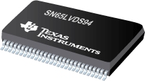
SN65LVDS94 - Serdes(串行器/解串器)接收器
SN65LVDS94是TI德州仪器公司的一款BLVDS/LVDS串行器/解串器(<100MHz)产品,SN65LVDS94是Serdes(串行器/解串器)接收器,本站介绍了SN65LVDS94的封装应用图解、特点和优点、功能等,并给出了与SN65LVDS94相关的TI元器件型号供参考。
SN65LVDS94 - Serdes(串行器/解串器)接收器 - BLVDS/LVDS串行器/解串器(<100MHz) - 串行器、解串器 - 德州仪器
The SN65LVDS94 LVDS serdes (serializer/deserializer) receiver contains four serial-in 7-bit parallel-out shift registers, a 7× clock synthesizer, and five low-voltage differential signaling (LVDS) line receivers in a single integrated circuit. These functions allow receipt of synchronous data from a compatible transmitter, such as the SN65LVDS93 and SN65LVDS95, over five balanced-pair conductors and expansion to 28 bits of single-ended LVTTL synchronous data at a lower transfer rate.
When receiving, the high-speed LVDS data is received and loaded into registers at the rate seven times the LVDS input clock (CLKIN). The data is then unloaded to a 28-bit wide LVTTL parallel bus at the CLKIN rate. A phase-locked loop clock synthesizer circuit generates a 7× clock for internal clocking and an output clock for the expanded data. The SN65LVDS94 presents valid data on the rising edge of the output clock (CLKOUT).
The SN65LVDS94 requires only five line termination resistors for the differential inputs and little or no control. The data bus appears the same at the input to the transmitter and output of the receiver with the data transmission transparent to the user(s). The only user intervention is the possible use of the shutdown/clear (SHTDN\) active-low input to inhibit the clock and shut off the LVDS receivers for lower power consumption. A low level on this signal clears all internal registers to a low level.
The SN65LVDS94 is characterized for operation over ambient air temperatures of -40°C to 85°C.
- 4:28 Data Channel Expansion at up to 1.904 Gigabits per Second Throughput
- Suited for Point-to-Point Subsystem Communication With Very Low EMI
- 4 Data Channels and Clock Low-Voltage Differential Channels in and 28 Data and Clock Out Low-Voltage TTL Channels Out
- Operates From a Single 3.3-V Supply and 250 mW (Typ)
- 5-V Tolerant SHTDN\ Input
- Rising Clock Edge Triggered Outputs
- Bus Pins Tolerate 4-kV HBM ESD
- Packaged in Thin Shrink Small-Outline Package With 20 Mil Terminal Pitch
- Consumes <1 mW When Disabled
- Wide Phase-Lock Input Frequency Range
- 20 MHz to 65 MHz
- No External Components Required for PLL
- Meets or Exceeds the Requirements of ANSI EIA/TIA-644 Standard
- Industrial Temperature Qualified TA = -40°C to 85°C
- Replacement for the DS90CR286
- TPS75003 - 面向 Xilinx(R) Spartan(TM)-3 FPGA 的集成三路电源管理 IC (PMIC)
- TSB41LV04A - IEEE 1394a 四端口电缆收发器/仲裁器
- FDC2212 - FDC2112 FDC2114
- CSD19534Q5A - 100V、N 通道 NexFET 功率 MOSFET,CSD19534Q5A
- TLC7705-EP - 增强型产品微功耗电源电压监控器
- TLV320AIC3253 - 具有 miniDSP 和立体声数字麦克风输入的超低功耗立体声音频编解码器
- LM3410 - 具有内部补偿的 525kHz/1.6MHz、恒流升压和 SEPIC LED 驱动器
- MSP430F4371 - 16 位超低功耗微控制器,具有 32kB 闪存、1024B RAM、USART 和 160 段 LCD
- OPA1662-Q1 - 汽车类 Sound Plus、低功耗、低噪声和低失真音频运算放大器
- TPS2086 - 0.7A 2.7 至 5.5V 四路(4 输入/4 输出)高侧 MOSFET 开关 IC,具有故障报告功能,2 个高电平有效启用,2 个低电平有效启用

