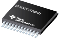

SN74AVC8T245-Q1是TI公司的一款方向控制电压转换产品,SN74AVC8T245-Q1是具有可配置电压转换和三态输出的汽车类 8 位双电源总线收发器,本页介绍了SN74AVC8T245-Q1的产品说明、应用、特性等,并给出了与SN74AVC8T245-Q1相关的TI元器件型号供参考。
SN74AVC8T245-Q1 - 具有可配置电压转换和三态输出的汽车类 8 位双电源总线收发器 - 方向控制电压转换 - 电压电平转换 - TI公司(Texas Instruments,德州仪器)
This 8-bit noninverting bus transceiver uses two separate configurable power-supply rails. The SN74AVC8T245 operation is optimimal with VCCA and VCCB set at 1.4 V to 3.6 V. It is operational with VCCA and VCCB as low as 1.2 V. The A port is designed to track VCCA. VCCA accepts any supply voltage from 1.2 V to 3.6 V. The B port is designed to track VCCB. VCCB accepts any supply voltage from 1.2 V to 3.6 V. This allows for universal low-voltage bidirectional translation between any of the 1.2-V, 1.5-V, 1.8-V, 2.5-V, and 3.3-V voltage nodes.
The SN74AVC8T245 design enables asynchronous communication between data buses. The device transmits data from the A bus to the B bus or from the B bus to the A bus, depending on the logic level at the direction-control (DIR) input. one can use the output-enable (OE) input to disable the outputs so the buses are effectively isolated.
In the SN74AVC8T245 design, VCCAsupplies the control pins (DIR and OE).
The SN74AVC8T245 solution is compatible with a single-supply system, which a ’245 function can replace later with minimal printed-circuit-board redesign.
This device specification covers partial-power-down applications using Ioff. The Ioff circuitry disables the outputs, preventing damaging current backflow through a powered-down device.
The VCC isolation feature ensures that if either VCC input is at GND, both ports are in the high-impedance state.
To ensure the high-impedance state during power up or power down, tie OE to VCC through a pullup resistor; the current-sinking capability of the driver determines the minimum value of the resistor.
- Qualified for Automotive Applications
- AEC Q100 Test Guidance With the Following Results:
- Device Temperature Grade 1: –40°C to 125°C Ambient Operating Temperature Range
- Device HBM ESD Classification Level H2
- Device CDM ESD Classification Level C3B
- Control Inputs VIH and VIL Levels Are Referenced to VCCA Voltage
- VCC Isolation Feature – If Either VCC Input Is at GND, All I/O Ports Are in the High-Impedance State
- Ioff Supports Partial Power-Down-Mode Operation
- Fully Configurable Dual-Rail Design Allows Each Port to Operate Over the Full 1.4-V to 3.6-V Power-Supply Range
- I/Os Are 4.6-V Tolerant
- Maximum Data Rates
- 170 Mbps (VCCA < 1.8 V or VCCB < 1.8 V)
- 320 Mbps (VCCA ≥ 1.8 V and VCCB ≥ 1.8 V)
- Latch-Up Performance Exceeds 100 mA per JESD 78, Class II


