


- LM26CIM5-SHA/NOPB - 传感器,变送器 > 温度传感器 > 温控器 - 固态
- LP2985IM5-3.6/NOPB - 集成电路(IC) > 电源管理(PMIC) > 稳压器 - 线性
- 74ACT11593NT - 集成电路(IC) > 逻辑 > 计数器,除法器
- TPS73601MDCQREP - 集成电路(IC) > 电源管理(PMIC) > 稳压器 - 线性
- SN74AHC1G86DBVRG4 - 集成电路(IC) > 逻辑 > 门和反相器
- TPS62400DRCT - 集成电路(IC) > 电源管理(PMIC) > 稳压器 - DC-DC 开关稳压器
- AM3358BZCE60 - 集成电路(IC) > 嵌入式 > 微处理器
- LP3933SL/NOPB - 集成电路(IC) > 电源管理(PMIC) > LED 驱动器
- PT4507N - 板安装电源 > 直流转换器
- LM5114AMFX/S7003103 - 集成电路(IC) > 电源管理(PMIC) > 栅极驱动器
- TMUX7211RUMR - 集成电路(IC) > 接口 > 模拟开关,多路复用器,解复用器
- PCA9554APW - 集成电路(IC) > 接口 > I/O 扩展器
- OPA2364IDGKT - 集成电路(IC) > 线性 > 放大器 > 仪器,运算放大器,缓冲器
- TPS2080EVM - 开发板,套件,编程器 > 评估板 > 评估和演示板及套件
- CDCVF855PWR - 集成电路(IC) > 时钟/定时 > 时钟发生器,PLL,频率合成器
- SN74ALVC244DWR - 集成电路(IC) > 逻辑 > 缓冲器,驱动器,接收器,收发器
- TPS62850120QDRLRQ1 - 集成电路(IC) > 电源管理(PMIC) > 稳压器 - DC-DC 开关稳压器
- 74FCT2543ATSOCTG4 - 逻辑 - 缓冲器,驱动器,接收器,收发器
- SN74LVCC3245APWR - 集成电路(IC) > 逻辑 > 转换器,电平移位器
- PT6477A - 直流转换器


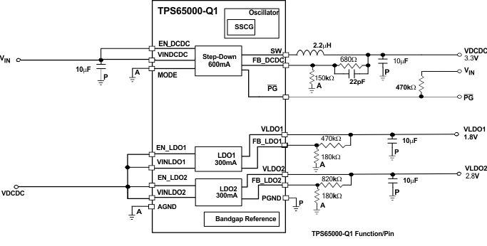
TPS65000-Q1 - 具有双路 LDO 和 SVS 的 2.25MHz 降压转换器
TPS65000-Q1是TI德州仪器公司的一款无产品,TPS65000-Q1是具有双路 LDO 和 SVS 的 2.25MHz 降压转换器,本站介绍了TPS65000-Q1的封装应用图解、特点和优点、功能等,并给出了与TPS65000-Q1相关的TI元器件型号供参考。
TPS65000-Q1 - 具有双路 LDO 和 SVS 的 2.25MHz 降压转换器 - 无 - 电源管理多通道IC(PMIC)解决方案 - 德州仪器
- Qualified for Automotive Applications
- AEC-Q100 Qualified With the Following Results:
- Device Temperature Grade 2: –40°C to +105°C Ambient Operating Temperature Range
- Device HBM ESD Classification Level H2
- Device CDM ESD Classification Level C4B
- Step-Down Converters:
- VIN Range From 2.3 V to 6 V
- Spread-Spectrum Clock (SSC) Generation for Reduced EMI
- 2.25-MHz Fixed-Frequency Operation
- 600-mA Output Current
- LDOs:
- VIN Range From 1.6 V to 6 V
- Adjustable Output Voltage
- Up to 300-mA Output Current
- Separate Power Inputs and Enables
- 3-mm × 3-mm 16-Pin QFN
- Automotive
- Point-of-Load
- Embedded Processor Power
- Cell Phones, Smart Phones
- PDAs, Pocket PCs
- Portable Media Players
The TPS65000-Q1 device is a single-chip power-management IC for portable applications. This device combines a single step-down converter with two low-dropout regulators. The step-down converter enters a low-power mode at light load for maximum efficiency across the widest possible range of load currents. For low-noise applications, the device can be forced into fixed-frequency PWM through a pin. The step-down converter allows the use of a small inductor and capacitors to achieve a small solution size. The step-down converter has a power-good status output that can be used for sequencing. The LDOs can supply 300 mA, and can operate with an input voltage range from 1.6 V tp 6 V, thus allowing them to be supplied from the step-down converter or directly from the main battery. The step-down converter and the LDOs have separate voltage inputs and enables, thus allowing for design and sequencing flexibility.
The TPS65000-Q1 is available in a 16-pin leadless package (3-mm × 3-mm QFN).
| PART NUMBER | PACKAGE | BODY SIZE (NOM) |
|---|---|---|
| TPS65000-Q1 | WQFN (16) | 3.00 mm × 3.00 mm |
- LM4673 - 免滤波、2.65W、单声道、D 类音频功率放大器
- DLPC3438 - 低功耗 DLP 显示控制器
- DAC7563T - DACxx6xT 16 位双路低功耗超低毛刺脉冲缓冲电压输出 DAC
- TL751M12-Q1 - 汽车类单路输出 LDO、750mA、固定电压 (12.0V)、使能端、60V 负载突降保护
- TPS53513 - 高性能、8A 单路同步降压转换器
- UC2524AM - 高级稳压脉宽调制器
- CLC007 - 具有双路补偿输出的串行数字电缆驱动器
- MSP430F157 - 16 位超低功耗 MCU,具有 32kB 闪存、1024B RAM、12 位 ADC、双 12 位 DAC、USART、I2C 和 DMA
- TLC6C5712-Q1 - TLC6C5712-Q1 12 位恒流下沉式 LED 驱动器
- ADC12EU050 - 超低功耗、八通道、12 位、45 MSPS Δ-Σ 模数转换器

